TMS320C6672
Multicore Fixed and Floating-Point Digital Signal Processor
SPRS708C—February 2012
www.ti.com
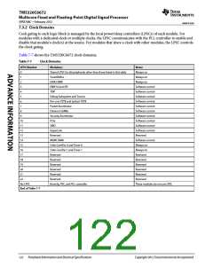
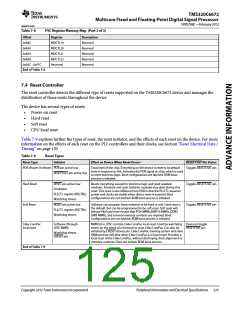
7.4.1 Power-on Reset
Power-on reset is used to reset the entire device, including the test and emulation logic.
Power-on reset is initiated by the following
1. POR pin
2. RESETFULL pin
During power-up, the POR pin must be asserted (driven low) until the power supplies have reached their normal
operating conditions. A RESETFULL pin is also provided to allow the on-board host to reset the entire device
including the reset isolated logic. The assumption is that, device is already powered up and hence unlike POR,
RESETFULL pin will be driven by the on-board host control other than the power good circuitry. For power-on
reset, the Main PLL Controller comes up in bypass mode and the PLL is not enabled. Other resets do not affect the
state of the PLL or the dividers in the PLL controller.
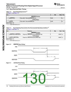
The following sequence must be followed during a power-on reset:
1. Wait for all power supplies to reach normal operating conditions while keeping the POR pin asserted (driven
low). While POR is asserted, all pins except RESETSTAT will be set to high-impedance. After the POR pin is
de-asserted (driven high), all Z group pins, low group pins, and high group pins are set to their reset state and
will remain at their reset state until otherwise configured by their respective peripheral. All peripherals that are
power managed, are disabled after a Power-on Reset and must be enabled through the Device State Control
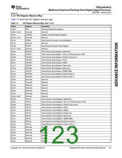
registers (for more details, see Section Table 3-2 ‘‘Device State Control Registers’’ on page 71).
2. Clocks are reset, and they are propagated throughout the chip to reset any logic that was using reset
synchronously. All logic is now reset and RESETSTAT will be driven low indicating that the device is in reset.
3. POR must be held active until all supplies on the board are stable then for at least an additional time for the
Chip level PLLs to lock.
4. The POR pin can now be de-asserted. Reset sampled pin values are latched at this point. The Chip level PLLs
is taken out of reset and begins its locking sequence, and all power-on device initialization also begins.
5. After device initialization is complete, the RESETSTAT pin is de-asserted (driven high). By this time, DDR3
PLL has already completed its locking sequence and is outputting a valid clock. The system clocks of both PLL
controllers are allowed to finish their current cycles and then paused for 10 cycles of their respective system
reference clocks. After the pause, the system clocks are restarted at their default divide by settings.
6. The device is now out of reset and device execution begins as dictated by the selected boot mode.
Note—To most of the device, reset is de-asserted only when the POR and RESET pins are both de-asserted
(driven high). Therefore, in the sequence described above, if the RESET pin is held low past the low period
of the POR pin, most of the device will remain in reset. The RESET pin should not be tied together with the
POR pin.
126
Peripheral Information and Electrical Specifications
Copyright 2012 Texas Instruments Incorporated

 TI [ TEXAS INSTRUMENTS ]