TMS320C6672
Multicore Fixed and Floating-Point Digital Signal Processor
SPRS708C—February 2012
www.ti.com
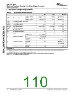
7.2.1 Power-Supply Sequencing
This section defines the requirements for a power up sequencing from a power-on reset condition. There are two
acceptable power sequences for the device. The first sequence stipulates the core voltages starting before the IO
voltages as shown below.
1. CVDD
2. CVDD1, VDDT1-3
3. DVDD18, AVDD1, AVDD2
4. DVDD15, VDDR1-4
The second sequence provides compatibility with other TI processors with the IO voltage starting before the core
voltages as shown below.
1. DVDD18, AVDD1, AVDD2
2. CVDD
3. CVDD1, VDDT1-3
4. DVDD15, VDDR1-4
The clock input buffers for CORECLK, DDRCLK, PASSCLK, SRIOSGMIICLK, PCIECLK and MCMCLK
use CVDD as a supply voltage. These clock inputs are not failsafe and must be held in a high-impedance state until
CVDD is at a valid voltage level. Driving these clock inputs high before CVDD is valid could cause damage to the
device. Once CVDD is valid it is acceptable that the P and N legs of these CLKs may be held in a static state (either
high and low or low and high) until a valid clock frequency is needed at that input. To avoid internal oscillation the
clock inputs should be removed from the high impedance state shortly after CVDD is present.
If a clock input is not used it must be held in a static state. To accomplish this the N leg should be pulled to ground
through a 1K ohm resistor. The P leg should be tied to CVDD to ensure it won't have any voltage present until
CVDD is active. Connections to the IO cells powered by DVDD18 and DVDD15 are not failsafe and should not be
driven high before these voltages are active. Driving these IO cells high before DVDD18 or DVDD15 are valid could
cause damage to the device.
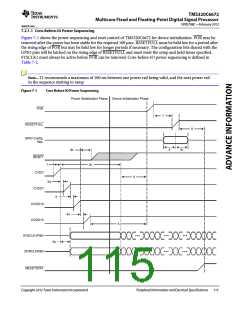
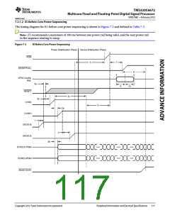
The device initialization is broken into two phases. The first phase consists of the time period from the activation of
the first power supply until the point in which all supplies are active and at a valid voltage level. Either of the
sequencing scenarios described above can be implemented during this phase. The figures below show both the
core-before-IO voltage sequence and the IO-before-core voltage sequence. POR must be held low for the entire
power stabilization phase.
This is followed by the device initialization phase. The rising edge of POR followed by the rising edge of RESETFULL
will trigger the end of the initialization phase but both must be inactive for the initialization to complete. POR must
always go inactive before RESETFULL goes inactive as described below. SYSCLK1 in the following section refers to
the clock that is used by the CorePac, see Figure 7-7 for more details.
114
Peripheral Information and Electrical Specifications
Copyright 2012 Texas Instruments Incorporated

 TI [ TEXAS INSTRUMENTS ]