TMS320C6672
Multicore Fixed and Floating-Point Digital Signal Processor
SPRS708C—February 2012
www.ti.com
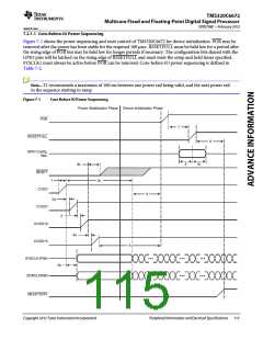
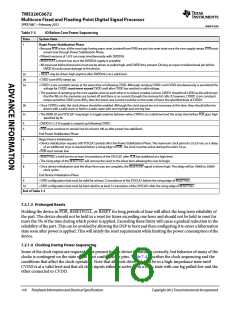
Table 7-3
IO Before Core Power Sequencing
Time
System State
Begin Power Stabilization Phase
1
• Because POR is low, all the core logic having async reset (created from POR) are put into reset state once the core supply ramps. POR must
remain low through Power Stabilization Phase.
• Filtered versions of 1.8 V can ramp simultaneously with DVDD18.
• RESETSTAT is driven low once the DVDD18 supply is available.
• All input and bidirectional pins must not be driven or pulled high until DVDD18 is present. Driving an input or bidirectional pin before
DVDD18 could cause damage to the device.
2a
2b
3a
• RESET may be driven high anytime after DVDD18 is at a valid level.
• CVDD (core AVS) ramps up.
• CVDD1 (core constant) ramps at the same time or following CVDD. Although ramping CVDD1 and CVDD simultaneously is permitted the
voltage for CVDD1 must never exceed CVDD until after CVDD has reached a valid voltage.
• The purpose of ramping up the core supplies close to each other is to reduce crowbar current. CVDD1 should trail CVDD as this will ensure
that the WLs in the memories are turned off and there is no current through the memory bit cells. If, however, CVDD1 (core constant)
ramps up before CVDD (core AVS), then the worst case current could be on the order of twice the specified draw of CVDD1.
3b
3c
• Once CVDD is valid, the clock drivers should be enabled. Although the clock inputs are not necessary at this time, they should either be
driven with a valid clock or held in a static state with one leg high and one leg low.
• The DDRCLK and SYSCLK1 may begin to toggle anytime between when CVDD is at a valid level and the setup time before POR goes high
specified by t6.
4
5
• DVDD15 (1.5 V) supply is ramped up following CVDD1.
• POR must continue to remain low for at least 100 μs after power has stabilized.
End Power Stabilization Phase
6
Begin Device Initialization
• Device initialization requires 500 SYSCLK1 periods after the Power Stabilization Phase. The maximum clock period is 33.33 nsec so a delay
of an additional 16 μs is required before a rising edge of POR. The clock must be active during the entire 16 μs.
• POR must remain low.
7
8
• RESETFULL is held low for at least 24 transitions of the SYSCLK1 after POR has stabilized at a high level.
• The rising edge of the RESETFULL will remove the reset to the efuse farm allowing the scan to begin.
• Once device initialization and the efuse farm scan are complete, the RESETSTAT signal is driven high. This delay will be 10000 to 50000
clock cycles.
End Device Initialization Phase
9
• GPIO configuration bits must be valid for at least 12 transitions of the SYSCLK1 before the rising edge of RESETFULL
• GPIO configuration bits must be held valid for at least 12 transitions of the SYSCLK1 after the rising edge of RESETFULL
10
End of Table 7-3
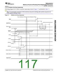
7.2.1.3 Prolonged Resets
Holding the device in POR, RESETFULL, or RESET for long periods of time will affect the long term reliability of
the part. The device should not be held in a reset for times exceeding one hour and should not be held in reset for
more the 5% of the time during which power is applied. Exceeding these limits will cause a gradual reduction in the
reliability of the part. This can be avoided by allowing the DSP to boot and then configuring it to enter a hibernation
state soon after power is applied. This will satisfy the reset requirement while limiting the power consumption of the
device.
7.2.1.4 Clocking During Power Sequencing
Some of the clock inputs are required to be present for the device to initialize correctly, but behavior of many of the
clocks is contingent on the state of the boot configuration pins. Table 7-4 describes the clock sequencing and the
conditions that affect the clock operation. Note that all clock drivers should be in a high-impedance state until
CVDD is at a valid level and that all clock inputs either be active or in a static state with one leg pulled low and the
other connected to CVDD.
118
Peripheral Information and Electrical Specifications
Copyright 2012 Texas Instruments Incorporated

 TI [ TEXAS INSTRUMENTS ]