TMP112
SBOS473B–MARCH 2009–REVISED JUNE 2009 ......................................................................................................................................................... www.ti.com
APPLICATION INFORMATION
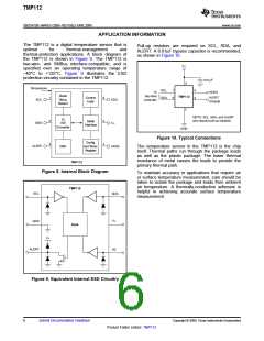
The TMP112 is a digital temperature sensor that is
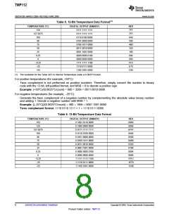
Pull-up resistors are required on SCL, SDA, and
optimal
for
thermal-management
and
ALERT. A 0.01µF bypass capacitor is recommended,
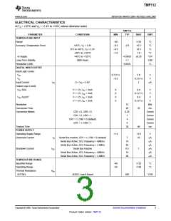
thermal-protection applications. A block diagram of
the TMP112 is shown in Figure 8. The TMP112 is
two-wire- and SMBus interface-compatible, and is
specified over an operating temperature range of
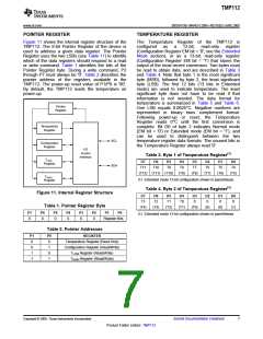
–40°C to +125°C. Figure 9 illustrates the ESD
protection circuitry contained in the TMP112.
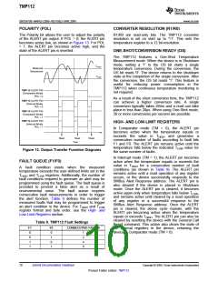
as shown in Figure 10.
V+
0.01mF
5
Temperature
SCL
SDA
1
6
4
3
To
Two-Wire
Controller
ADD0
Diode
TMP112
ALERT
1
2
3
Control
Logic
6
5
4
Temp.
SCL
GND
SDA
(Output)
Sensor
2
NOTE: SCL, SDA, and ALERT
pins require pull-up resistors.
DS
A/D
Serial
V+
Interface
Converter
GND
Figure 10. Typical Connections
Config.
and Temp.
Register
ALERT
OSC
ADD0
The temperature sensor in the TMP112 is the chip
itself. Thermal paths run through the package leads
as well as the plastic package. The lower thermal
resistance of metal causes the leads to provide the
primary thermal path.
TMP112
Figure 8. Internal Block Diagram
To maintain accuracy in applications that require air
or surface temperature measurement, care should be
taken to isolate the package and leads from ambient
air temperature. A thermally-conductive adhesive is
helpful in achieving accurate surface temperature
measurement.
TMP112
SCL
SDA
V+
GND
Core
V+
ALERT
A0
Figure 9. Equivalent Internal ESD Circuitry
6
Submit Documentation Feedback
Copyright © 2009, Texas Instruments Incorporated
Product Folder Link(s): TMP112

 TI [ TEXAS INSTRUMENTS ]