TMP112
SBOS473B–MARCH 2009–REVISED JUNE 2009 ......................................................................................................................................................... www.ti.com
This integrated circuit can be damaged by ESD. Texas Instruments recommends that all integrated circuits be handled with
appropriate precautions. Failure to observe proper handling and installation procedures can cause damage.
ESD damage can range from subtle performance degradation to complete device failure. Precision integrated circuits may be more
susceptible to damage because very small parametric changes could cause the device not to meet its published specifications.
PACKAGE INFORMATION(1)
PRODUCT
PACKAGE-LEAD
PACKAGE DESIGNATOR
PACKAGE MARKING
TMP112
SOT563
DRL
OBS
(1) For the most current package and ordering information, see the Package Option Addendum at the end of this document, or see the TI
web site at www.ti.com.
ABSOLUTE MAXIMUM RATINGS(1)
PARAMETER
TMP112
5
UNIT
V
Supply Voltage
Input Voltage, Pins 1, 4, and 6
Input Voltage, Pin 3
Operating Temperature
Storage Temperature
Junction Temperature
–0.5 to +5
–0.5 to (VS) + 0.5
–55 to +150
–60 to +150
+150
V
V
°C
°C
°C
V
Human Body Model (HBM)
2000
ESD Rating
Charged Device Model (CDM)
Machine Model (MM)
1000
V
200
V
(1) Stresses above these ratings may cause permanent damage. Exposure to absolute maximum conditions for extended periods may
degrade device reliability. These are stress ratings only, and functional operation of the device at these or any other conditions beyond
those specified is not supported.
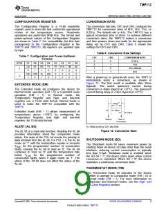
PIN CONFIGURATION
DRL PACKAGE
SOT563
(TOP VIEW)
SCL
GND
1
2
3
6
5
4
SDA
V+
ALERT
ADD0
2
Submit Documentation Feedback
Copyright © 2009, Texas Instruments Incorporated
Product Folder Link(s): TMP112

 TI [ TEXAS INSTRUMENTS ]