TMDS361
www.ti.com ............................................................................................................................................................................................ SLLS919–DECEMBER 2008
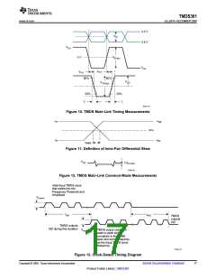
3.3 V
VID
2.8 V
VID+
VID(pp)
0 V
VID–
tPLH
tPHL
80%
80%
VOD(pp)
VOD
20%
20%
tr
tf
T0391-01
Figure 10. TMDS Main-Link Timing Measurements
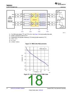
V
OH
V
Y
50%
V
Z
V
OL
t
sk(D)
Figure 11. Definition of Intra-Pair Differential Skew
VOC
DVOC(SS)
T0392-01
Figure 12. TMDS Main-Link Common-Mode Measurements
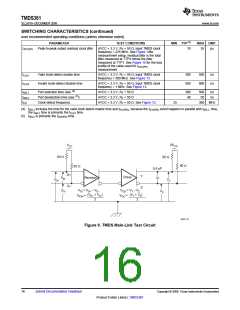
Valid Input TMDS clock
that meets the min
Frequency Threshold and
Amplitude
VCD(PP)
tclk1
tclk2
TMDS
outputs
HiZ
TMDS outputs
HiZ during this duration
TMDS output clock with
peak to peak swing
compliant to the HDMI
spec and same frequency
as the Input TMDS clock
frequency
VOD(PP)
T0424-01
Figure 13. Clock-Detect Timing Diagram
Copyright © 2008, Texas Instruments Incorporated
Submit Documentation Feedback
17
Product Folder Link(s) :TMDS361

 TI [ TEXAS INSTRUMENTS ]