ꢀ ꢁꢂ ꢃ ꢄꢅ ꢆꢇ ꢈ ꢉꢉ ꢅꢃ
SLAS356 − DECEMBER 2001
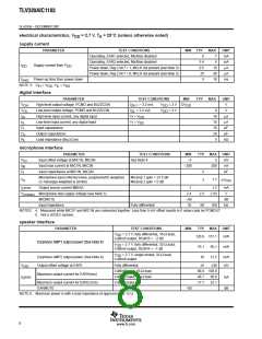
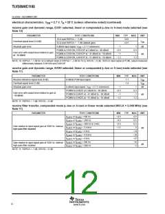
electrical characteristics, V
= 2.7 V, T = 25°C (unless otherwise noted)
DD
A
supply current
PARAMETER
TEST CONDITIONS
MIN TYP
MAX
UNIT
mA
mA
µA
Operating, EAR1 selected, MicBias disabled
6
7
Operating, EAR2 selected, MicBias disabled
5.4
0.5
25
5
6
10
40
10
I
t
Supply current from V
DD
DD
Power down, Reg 2 bit 7 = 1, MCLK not present (see Note 3)
Power down, Reg 2 bit 7 = 0, MCLK not present (see Note 3)
µA
Power-up time from power down
ms
on(i)
NOTE 3:
V = V , V = V
IH DD IL SS
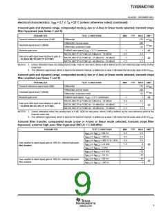
digital interface
PARAMETER
TEST CONDITIONS
MIN
TYP
MAX
UNIT
V
V
V
High-level output voltage, PCMO and BUZZCON
Low-level output voltage, PCMO and BUZZCON
High-level input current, any digital input
Low-level input current, any digital input
Input capacitance
I
I
= −3.2 mA,
= 3.2 mA,
V
= 3 V DV
DD
OH
OH
DD
DD
V
= 3 V
0
10
10
10
20
5
V
OL
OL
I
I
V = V
µA
µA
pF
pF
kΩ
IH
I
DD
V = V
IL
I
SS
C
C
R
I
Output capacitance
o
L
Load impedance (BuzzCon)
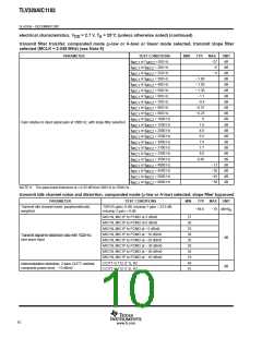
microphone interface
PARAMETER
TEST CONDITIONS
MIN
−5
TYP
MAX
5
UNIT
mV
nA
V
IO
Input offset voltage at MIC1N, MIC2N
Input bias current at MIC1N, MIC2N
Input capacitance at MIC1N, MIC2N
See Note 4
I
IB
−200
200
C
5
3
pF
i
Microphone input referred noise, psophometric weighted
(C-message weighted is similar)
Micamp 1 gain = 23.5 dB
Micamp 2 gain = 0 dB
V
n
7.7 µV
rms
I
max
Output source current MBIAS
Microphone bias supply voltage (see Note 5)
MICMUTE
1
2.4
−80
35
1.2
mA
O
V
2.5
60
2.55
V
(mbias)
dB
kΩ
Input impedance
Fully differential
100
NOTES: 4. Measured while MIC1P and MIC1N are connected together. Less than 5-mV offset results in 0 value code on PCMOUT.
5. Not a JEDEC symbol.
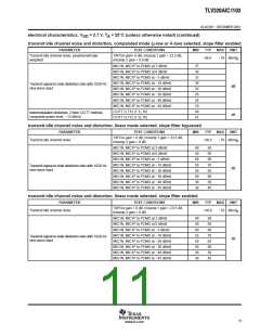
speaker interface
PARAMETER
TEST CONDITIONS
MIN
TYP
MAX
UNIT
V
= 2.7 V, fully differential, 16-Ω load,
DD
120.9 151.1
mW
3-dBm0 output, RGXPA = −2 dB
Earphone AMP1 output power (See Note 6)
V
= 2.7 V, fully differential, 32-Ω load,
DD
3-dBm0 output, RGXPA = −1 dB
76.1
95.1
mW
V
= 2.7 V, single ended, 32-Ω load,
DD
Earphone AMP2 output power (See Note 6)
Output offset voltage at EAR1
10
5
12.5
30
mW
mV
3-dBm0 output
V
OO
Fully differential
3-dBm0 input, 16-Ω load
3-dBm0 input, 32-Ω load
3-dBm0 input
86.9 108.6
Maximum output current for EAR1(rms)
48.7
17.7
60.8
22.1
I
max
mA
dB
O
Maximum output current for EAR2 (rms)
EARMUTE
−80
NOTE 6: Maximum power is with a load impedance of approximately 12 Ω.
8
www.ti.com

 TI [ TEXAS INSTRUMENTS ]