ꢀ ꢁꢂ ꢃ ꢄꢅ ꢆꢇ ꢈ ꢉꢉ ꢅꢃ
SLAS356 − DECEMBER 2001
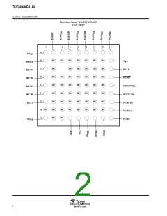
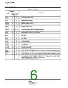
Terminal Functions
TERMINAL
NO.
I/O
DESCRIPTION
NAME
µBGA
PBS
32
8
AV
AV
A1
J1
F9
J6
J7
A6
A4
A2
A5
I
I
Analog positive power supply
Analog negative power supply
DD
SS
BUZZCON
19
13
14
27
29
31
28
O
I
Buzzer output, a pulse-density modulated signal to apply to external buzzer driver
Digital positive power supply
DV
DV
DD
SS
I
Digital negative power supply
Earphone 1 amplifier output (−)
Earphone 1 amplifier output (+)
Earphone 2 amplifier output
EAR1ON
EAR1OP
EAR2O
O
O
O
I
EARV
Analog positive power supply for the earphone amplifiers
Analog negative power supply for the earphone amplifiers
Microphone bias supply output, no decoupling capacitors
Master system clock input (2.048 MHz) (digital)
MIC1 input (+)
DD
SS
EARV
A3, A7 30, 26
I
MBIAS
MCLK
B1
C9
C1
D1
E1
F1
J8
1
O
I
22
2
MIC1P
MIC1N
MIC2P
MIC2N
PCMI
I
3
I
MIC1 input (−)
4
I
MIC2 input (+)
5
I
MIC2 input (−)
15
16
18
17
24
25
20
6
I
Receive PCM input
PCMO
PCMSYN
PCMCLK
J9
O
I
Transmit PCM output
G9
H9
A9
A8
E9
G1
D9
J5
PCM frame synchronization
I
PCM data clock
PLLV
PLLV
I
PLL negative power supply
SS
I
PLL digital power supply
DD
PWRUPSEL
REXT
I
Selects the power-up default mode
I/O Internal reference current setting terminal—use precision 100-kΩ resistor and no filtering capacitors
RESET
SCL
21
12
11
I
I
Active low reset
2
I C-bus serial clock—this input is used to synchronize the data transfer from and to the PCM codec
2
SDA
J4
I/O I C-bus serial address/data input/output—this is a bidirectional terminal used to transfer register
control addresses and data into and out of the CODEC. It is an open-drain terminal and therefore
requires a pullup resistor to V
DD
(typical 10 kΩ for 100 kHz)
V
SS
B9
23
I
Ground return for bandgap internal reference
6
www.ti.com

 TI [ TEXAS INSTRUMENTS ]