ꢀ ꢁꢂꢃ ꢄ ꢅ ꢆꢇ ꢈꢉꢉꢅ ꢃ
SLAS356 − DECEMBER 2001
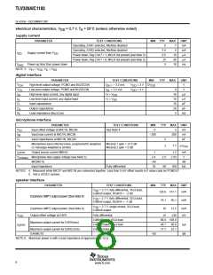
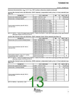
electrical characteristics, V
= 2.7 V, T = 25°C (unless otherwise noted) (continued)
A
DD
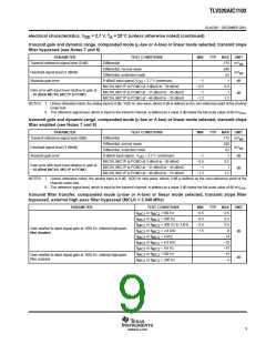
transmit gain and dynamic range, companded mode (µ-law or A-law) or linear mode selected, transmit slope
filter bypassed (see Notes 7 and 8)
PARAMETER
TEST CONDITIONS
MIN
TYP
MAX
UNIT
Transmit reference-signal level (0 dB)
Differential
175 mV
pp
Differential, normal mode
Differential, extended mode
248
63
1
Overload-signal level (3 dBm0)
Absolute gain error
mV
pp
0-dBm0 input signal, V
DD
= 2.7 V (minimum)
−1
−0.5
−1
dB
MIC1N, MIC1P to PCMO at 3 dBm0 to −30 dBm0
MIC1N, MIC1P to PCMO at −31 dBm0 to −45 dBm0
MIC1N, MIC1P to PCMO at −46 dBm0 to −55 dBm0
0.5
1
Gain error with input level relative to gain at
−10 dBm0 MIC1N, MIC1P to PCMO
dB
−1.2
1.2
NOTES: 7. Unless otherwise noted, the analog input is 0 dB, 1020-Hz sine wave, where 0 dB is defined as the zero-reference point of the channel
under test.
8. The reference signal level, which is input to the transmit channel, is defined as a value 3 dB below the full-scale value of 88-mV
.
rms
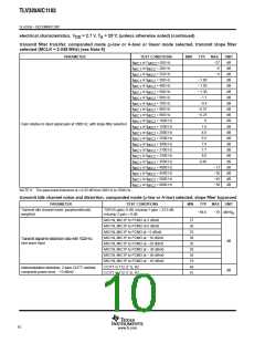
transmit gain and dynamic range, companded mode (µ-law or A-law) or linear mode selected, transmit slope
filter enabled (see Notes 7 and 8)
PARAMETER
TEST CONDITIONS
MIN
TYP
MAX
UNIT
Transmit reference-signal level (0dB)
Differential
175 mV
pp
Differential, normal mode
Differential, extended mode
248
63
1
Overload-signal level (3 dBm0)
Absolute gain error
mV
pp
0-dBm0 input signal, V
DD
= 2.7 V (minimum)
−1
−0.5
−1
dB
MIC1N, MIC1P to PCMO at 3 dBm0 to −30 dBm0
MIC1N, MIC1P to PCMO at −31 dBm0 to −45 dBm0
MIC1N, MIC1P to PCMO at −46 dBm0 to −55 dBm0
0.5
1
Gain error with input level relative to gain at
−10-dBm0 MIC1N, MIC1P to PCMO
dB
−1.2
1.2
NOTES: 7. Unless otherwise noted, the analog input is 0 dB, 1020-Hz sine wave, where 0 dB is defined as the zero-reference point of the
channel under test.
8. The reference signal level, which is input to the transmit channel, is defined as a value 3 dB below the full-scale value of 88-mV
rms
.
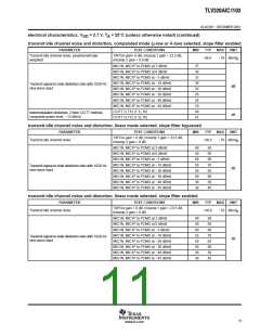
transmit filter transfer, companded mode (µ-law or A-law) or linear mode selected, transmit slope filter
bypassed, external high pass filter bypassed (MCLK = 2.048 MHz)
PARAMETER
TEST CONDITIONS
MIN
−0.5
−0.5
−0.5
−1.5
TYP
MAX
0.5
UNIT
f
f
f
f
f
f
f
f
f
or f
or f
or f
or f
or f
or f
or f
or f
or f
<100 Hz
MIC1
MIC1
MIC1
MIC1
MIC1
MIC1
MIC1
MIC1
MIC1
MIC2
MIC2
MIC2
MIC2
MIC2
MIC2
MIC2
MIC2
MIC2
= 200 Hz
= 300 Hz to 3 kHz
= 3.4 kHz
= 4 kHz
0.5
0.5
Gain relative to input signal gain at 1020 Hz, internal high-pass
filter disabled
0
dB
−14
−35
−47
−15
−5
= 4.6 kHz
= 8 k Hz
<100 Hz
Gain relative to input signal gain at 1020 Hz, internal high-pass
filter enabled
dB
= 200 Hz
9
www.ti.com

 TI [ TEXAS INSTRUMENTS ]