ꢀ ꢁꢂꢃ ꢄ ꢅ ꢆꢇ ꢈꢉꢉꢅ ꢃ
SLAS356 − DECEMBER 2001
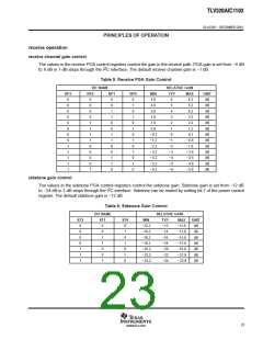
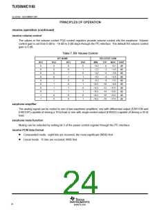
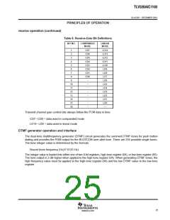
PRINCIPLES OF OPERATION
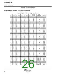
DTMF generator operation and interface (continued)
Tones from the DTMF generator block are present at all outputs and are controlled by enabling or disabling the
individual output ports. The values that determine the tone frequency are loaded into the tone registers (high
and low) as two separate values.
The values loaded into the tone registers initiate an iterative table look-up function, placing a 6 bit or 7 bit in twos
complement value into the the tone registers. There is a 2 dB difference in the resulting output of the two
registers, the high-tone register having the greater result.
The resulting range of a tone set into the low register value is +31 {1F}HEX to −32 {20}HEX for a range of six
bits and is in twos complement format. The resulting range of a tone set into the high register value is +39
{27}HEX to −40 {D8}HEX in twos-complement format, as well.
The maximum range is six bits having a maximum value of {31}HEX. The value {31} is represented as 011111.
Two zeros are added to the leading side of the value and then the value is padded with seven LSB zeros to create
a value of 000 1111 1000 0000. Because the maximum full scale value is 000 1111 1000 0000, the resulting
output magnitude is 20 log (input value/maximum value) or 20 log (3968/16783) or −12.31 dB below full scale.
This is the result when all gains are set at default.
buzzer logic section
The single-ended output BUZZCON is a PDM signal intended to drive a buzzer through an external driver
transistor. The PDM begins as a selected tone, is generated and passed through the receive D/A channel, and
is fed back to the transmit channel analog modulator, where a PDM signal is generated and routed to the
BUZZCON output.
support section
The clock generator and control circuit uses the master clock input (MCLK) to generate internal clocks to drive
internal counters, filters, and converters. Register control data is written into and read back from the VBAP
registers via the control interface.
2
I C-bus protocols
2
The PCM codec serial interface is designed to be I C bus-compatible and operates in the slave mode. This
interface consists of the following terminals:
2
SCL: I C bus serial clock—This input synchronizes the control data transfer from and to the CODEC.
2
SDA: I C bus serial address/data input/output—This is a bidirectional terminal that transfers register
control addresses and data into and out of the codec. It is an open drain terminal and therefore
requires a pullup resistor to V
(typical 10 kΩ for 100 kHz).
CC
TLV320AIC1103 has a fixed device select address of {E2}HEX for write mode and {E3}HEX for read mode.
For normal data transfer, SDA is allowed to change only when SCL is low. Changes when SCL is high are
reserved for indicating the start and stop conditions.
Data transfer may be initiated only when the bus is not busy. During data transfer, the data line must remain
stable whenever the clock line is at high. Changes in the data line while the clock line is at high are interpreted
as a start or stop condition.
27
www.ti.com

 TI [ TEXAS INSTRUMENTS ]