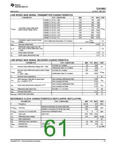
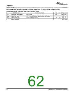
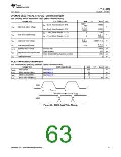
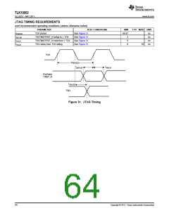
TLK10002
www.ti.com
SLLSE75 –MAY 2011
POWER SEQUENCING GUIDELINES
The TLK10002 allows either the core or I/O power supply to be powered up for an indefinite period of time while
the other supply is not powered up, if all of the following conditions are met:
1. All maximum ratings and recommended operating conditions are followed.
2. Bus contention while 1.5V/1.8V power is applied (>0V) must be limited to 100 hours over the projected
lifetime of the device.
3. Junction temperature is less than 105°C during device operation. Note: Voltage stress up to the absolute
maximum voltage values for up to 100 hours of lifetime operation at a junction temperature of 105°C or lower
will minimally impact reliability.
The TLK10002 inputs are not failsafe (i.e., cannot be driven with the I/O power disabled). TLK10002 inputs
should not be driven high until their associated power supplies are active.
DEVICE INITIALIZATION
The following sequence should be performed to initialize and ensure proper operation of the TLK10002 device.
This procedure is optimized for electrical connection on HS serial side.
4:1 Mode (9.8304Gbps on HS side, 2.4576Gbps per lane on LS side)
Note: Assume both channel A and channel B have the same setup.
REFCLK frequency = 122.88MHz, Mode = Transceiver, 4 to 1 serialization on LS side inputs and 1 to 4
deserialization on HS side inputs.
•
Device Pin Setting(s) – Pin settings allow for maximum software configurability.
–
–
–
–
–
Ensure PD_TRXA_N input pin is High.
Ensure PD_TRXB_N input pin is High.
Ensure PRBSEN input pin is Low.
Ensure REFCLKA_SEL input pin is Low to enable software control.
Ensure REFCLKB_SEL input pin is Low to enable software control.
•
Reset Device
–
Issue a hard or soft reset (RESET_N asserted for at least 10 µs -or- Write 1’b1 to 0.15 GLOBAL_RESET)
after power supply stabilization.
•
•
Enable MDIO global write so that each MDIO write affects both channels to shorten provisioning time
Write 1’b1 to 0.11 GLOBAL_WRITE
Clock Configuration and Mode control
–
–
–
–
Write 1’b1 to 1.9 RX_DEMUX_SEL to select 1 to 4 on the receive side
Write 1’b1 to 1.8 TX_MUX_SEL to select 4 to 1 on the transmit side
Select respective Channel SERDES REFCLK input (Default = REFCLK0P/N)
–
–
If REFCLK0P/N used – Write 1’b0 to 1.1 REFCLK_ SEL
If REFCLK1P/N used – Write 1’b1 to 1.1 REFCLK_ SEL
•
HS/LS Data Rate Setting (Refer to Table 4 for more CPRI/OBSAI Rates)
–
Write 4’b1101 to 2.3:0 HS_PLL_MULT[3:0], write 2’b00 to 3.9:8 HS_RATE_RX[1:0], write 2’b00 to 3.1:0
HS_RATE_TX[1:0], to select FULL rate and 20x MPY on HS side (HS_SERDES_CONTROL_1 = 0x811D,
HS_SERDES_CONTROL_2 = 0xA444).
–
–
Write 1'B1 to 9.9 HS_PEAK_DISABLE (HS_OVERLAY_CONTROL = 0x0B00).
Write 4’b0101 to 6.3:0 LS_MPY[3:0], write 2’b00 to 7.9:8 LS_IN_RATE[1:0], write 2’b00 to 7.1:0
LS_OUT_RATE [1:0], to select FULL rate and 10x MPY on LS side (LS_SERDES_CONTROL_1 =
0xF115, LS_SERDES_CONTROL_2 = 0xDC04).
•
HS Serial Configuration
Configure the following bits per the desired application:
–
–
–
–
2.9:8 (HS_LOOP_BANDWIDTH[1:0]), 2.6 (HS_VRANGE)
3.15:12 (HS_SWING[3:0]), 3.7:6 (HS_AGCCTRL[1:0])
3.5:4 (HS_AZCAL[1:0]), 4.14:12 (HS_EQPRE[2:0])
Copyright © 2011, Texas Instruments Incorporated
65

 TI [ TEXAS INSTRUMENTS ]