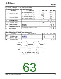
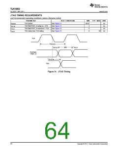
TLK10002
www.ti.com
SLLSE75 –MAY 2011
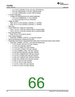
2:1 Mode (9.8304Gbps on HS side, 4.9152Gbps per lane on LS side, Only Lanes 0 and 1 on LS
side active)
Note: Assume both channel A and channel B have the same setup.
REFCLK frequency = 122.88MHz, Mode = Transceiver, 2 to 1 serialization on LS side inputs and 1 to 2
deserialization on HS side inputs.
•
Device Pin Setting(s) – Pin settings allow for maximum software configurability.
–
–
–
–
–
Ensure PD_TRXA_N input pin is High.
Ensure PD_TRXB_N input pin is High.
Ensure PRBSEN input pin is Low.
Ensure REFCLKA_SEL input pin is Low to enable software control.
Ensure REFCLKB_SEL input pin is Low to enable software control.
•
Reset Device
–
Issue a hard or soft reset (RESET_N asserted for at least 10 µs -or- Write 1’b1 to 0.15 GLOBAL_RESET)
after power supply stabilization.
•
•
Enable MDIO global write so that each MDIO write affects both channels to shorten provisioning time
Write 1’b1 to 0.11 GLOBAL_WRITE
Clock Configuration and Mode control
–
–
–
–
Write 1’b0 to 1.9 RX_DEMUX_SEL to select 1 to 2 on the receive side
Write 1’b0 to 1.8 TX_MUX_SEL to select 2 to 1 on the transmit side
Select respective Channel SERDES REFCLK input (Default = REFCLK0P/N)
–
–
If REFCLK0P/N used – Write 1’b0 to 1.1 REFCLK_ SEL
If REFCLK1P/N used – Write 1’b1 to 1.1 REFCLK_ SEL
•
HS/LS Data Rate Setting (Refer to Table 4 for more CPRI/OBSAI Rates)
–
Write 4’b1101 to 2.3:0 HS_PLL_MULT[3:0], write 2’b00 to 3.9:8 HS_RATE_RX[1:0], write 2’b00 to 3.1:0
HS_RATE_TX[1:0], to select FULL rate and 20x MPY on HS side (HS_SERDES_CONTROL_1 = 0x811D,
HS_SERDES_CONTROL_2 = 0xA444).
–
–
Write 1'b1 to 9.9 HS_PEAK_DISABLE (HS_OVERLAY_CONTROL = 0x0B00)
Write 4’b1001 to 6.3:0 LS_MPY[3:0], write 2’b00 to 7.9:8 LS_IN_RATE[1:0], write 2’b00 to 7.1:0
LS_OUT_RATE [1:0], to select FULL rate and 20x MPY on LS side (LS_SERDES_CONTROL_1 =
0XF119, LS_SERDES_CONTROL_2 = 0xDC04).
•
HS Serial Configuration
Configure the following bits per the desired application:
–
–
–
–
–
–
–
2.9:8 (HS_LOOP_BANDWIDTH[1:0]), 2.6 (HS_VRANGE)
3.15:12 (HS_SWING[3:0]), 3.7:6 (HS_AGCCTRL[1:0])
3.5:4 (HS_AZCAL[1:0]), 4.14:12 (HS_EQPRE[2:0])
4.11:10 (HS_CDRFMULT[1:0]), 4.9:8 (HS_CDRTHR[1:0])
4.4:0 (HS_TWCRF[4:0]), 5.12:8 (HS_TWPOST1[4:0])
5.7:4 (HS_TWPRE[3:0]), 5.3:0 (HS_TWPOST2[3:0])
•
•
LS Serial Configuration
Configure the following bits per the desired application:
–
–
–
7.14:12 (LS_SWING[2:0]), 7.7:4 (LS_DE[3:0])
8.11:8 (LS_EQ [3:0]), 8.6:4 (LS_CDR [2:0])
Toggle HS_ENRX
–
–
Write 1'b0 to 3.2 (HS_SERDES_CONTROL_2 = 0xA440)
Write 1'b1 to 3.2 (HS_SERDES_CONTROL_2 = 0xA444)
•
•
Wait 10ms
Check SERDES PLL Status for Locked State
–
–
Poll F.1 LS_PLL_LOCK (per channel) until it is asserted (high)
Poll F.0 HS_PLL_LOCK (per channel) until it is asserted (high)
•
Issue Data path Reset
Copyright © 2011, Texas Instruments Incorporated
67

 TI [ TEXAS INSTRUMENTS ]