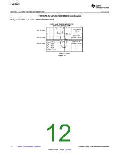
TLC5928
SBVS120A–JULY 2008–REVISED SEPTEMBER 2008 ................................................................................................................................................. www.ti.com
LED OPEN DETECTION (LOD) AND PRE-THERMAL WARNING (PTW)
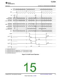
The LED open detection (LOD) circuit checks the voltage of each active (that is, on) constant current sink output
(OUT0 through OUT15) to detect open LEDs and LEDs shorted to GND while BLANK is low. The LOD bits in the
status information data register (SID) are set to '1' if the voltage of the corresponding OUTn pin is less than the
LED open detection threshold (VLOD = 0.3 V, typ). The status information data can be read from the SOUT pin.
To avoid false detection of open LEDs, the LED driver design must ensure that the constant-current sink output
voltage is greater than 0.3 V when the outputs are on. Also, the output on-time must be 1 µs or greater to
correctly read the valid LOD status.
The PTW function indicates that the IC junction temperature is too high. The PTW bit in the SID data is set to '1'
while the IC junction temperature exceeds the temperature threshold (T(PTW) = +138 °C, typ). If the IC junction
temperature decreases below the temperature of T(PTW), the SID data are set depending on the LOD function.
The constant current outputs are not forced off during PTW conditions, so the controller should take appropriate
action (such as reducing the duty cycle of effected channels).
The LOD and PTW data are latched into the SID latch with the rising edge of BLANK and do not change until
BLANK goes low. The SID data latched in the latch are transferred into the on/off shift register with a rising edge
of LAT. SID can be shifted out from SOUT with rising edges of SCLK. The data in the on/off control shift register
are replaced with the LOD and PTW data at the rising edge of LAT. Therefore, LAT should be input only once
after the shift data are updated to avoid the on/off control data latch information from being replaced with LOD
and PTW data in the shift register. A timing diagram for LOD, PTW, and SID is shown in Figure 19.
BLANK
OUTn OFF
OUTn
OUTn ON
VOUTn
If the voltage of OUTn (VOUTn) is less than VLOD (0.3 V, typ) when OUTn is on,
GND
then the LOD circuit reports error information to the LOD data latch
and the error information is set as '1' to the bit that corresponds with
the error OUTn in the LOD data latch.
LOD circuit needs 1ms to detect LED
open correctly as maximum.
LOD Circuit Data
(Internal)
Latest Error Information From LOD Circuit
No Error Information
No Error Information
LOD and PTW data are always copied into
SID data latch while BLANK is low level.
TJ < T(PTW)
:
TJ < T(PTW)
:
PTW Circuit Data
(Internal)
Normal Temperature
Normal Temperature
TJ ³ T(PTW): High Temperature
LOD and PTW data of from before
BLANK goes high are held in the
SID data latch at the rising edge of BLANK.
Previous LOD and PTW Data
SID Data Latch
(Internal)
PTW Error
Latest Error Information From LOD and PTW Circuit
No Error Information
Figure 19. LOD/PTW/SID timing
16
Submit Documentation Feedback
Copyright © 2008, Texas Instruments Incorporated
Product Folder Link(s): TLC5928

 TI [ TEXAS INSTRUMENTS ]