TCA9517
www.ti.com
SCPS242 –DECEMBER 2012
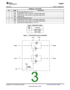
TERMINAL FUNCTIONS
NO.
1
NAME
VCCA
SCLA
SDAA
GND
EN
DESCRIPTION
A-side supply voltage (0.9 V to 5.5 V)
2
Serial clock bus, A side. Connect to VCCA through a pullup resistor.
Serial data bus, A side. Connect to VCCA through a pullup resistor.
Supply ground
3
4
5
Active-high repeater enable input
6
SDAB
SCLB
VCCB
Serial data bus, B side. Connect to VCCB through a pullup resistor.
Serial clock bus, B side. Connect to VCCB through a pullup resistor.
B-side and device supply voltage (2.7 V to 5.5 V)
7
8
Table 1. FUNCTION TABLE
INPUT
FUNCTION
EN
L
Outputs disabled
SDAA = SDAB
SCLA = SCLB
H
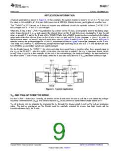
Figure 1. FUNCTIONAL BLOCK DIAGRAM
V
V
CCB
CCA
1
8
6
3
SDAA
SDAB
7
2
SCLA
SCLB
V
CCB
Pullup
Resistor
5
EN
4
GND
Copyright © 2012, Texas Instruments Incorporated
Submit Documentation Feedback
3
Product Folder Links: TCA9517

 TI [ TEXAS INSTRUMENTS ]