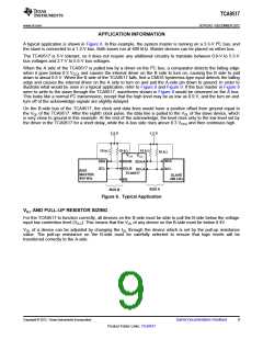
TCA9517
SCPS242 –DECEMBER 2012
www.ti.com
This integrated circuit can be damaged by ESD. Texas Instruments recommends that all integrated circuits be handled with
appropriate precautions. Failure to observe proper handling and installation procedures can cause damage.
ESD damage can range from subtle performance degradation to complete device failure. Precision integrated circuits may be more
susceptible to damage because very small parametric changes could cause the device not to meet its published specifications.
DESCRIPTION/ORDERING INFORMATION (CONTINUED)
The B-side drivers operate from 2.7 V to 5.5 V and behave like the drivers in the PCA9515A. The output low
level for this internal buffer is approximately 0.5 V, but the input voltage must be 70 mV or more below the output
low level when the output internally is driven low. The higher-voltage low signal is called a buffered low. When
the B-side I/O is driven low internally, the low is not recognized as a low by the input. This feature prevents a
lockup condition from occurring when the input low condition is released.
This type of design on the B side prevents it from being used in series with the PCA9515A and another TCA9517
(B side). This is because these devices do not recognize buffered low signals as a valid low and do not
propagate it as a buffered low again.
The A-side drivers operate from 0.9 V to 5.5 V and drive more current. They do not require the buffered low
feature (or the static offset voltage). This means that a low signal on the B side translates to a nearly 0-V low on
the A side, which accommodates smaller voltage swings of lower-voltage logic. The output pulldown on the
A side drives a hard low, and the input level is set at 0.3 VCCA to accommodate the need for a lower low level in
systems where the low-voltage-side supply voltage is as low as 0.9 V.
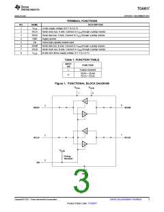
The A side of two or more TCA9517s can be connected together to allow a star topography, with the A side on
the common bus. Also, the A side can be connected directly to any other buffer with static- or dynamic-offset
voltage. Multiple TCA9517s can be connected in series, A side to B side, with no buildup in offset voltage and
with only time-of-flight delays to consider.
The TCA9517 drivers are enabled when VCCA is above 0.8 V and VCCB is above 2.5 V.
The TCA9517 has an active-high enable (EN) input with an internal pullup to VCCB, which allows the user to
select when the repeater is active. This can be used to isolate a badly behaved slave on power-up reset. The EN
input should change state only when the global bus and repeater port are in an idle state, to prevent system
failures.
The TCA9517 includes a power-up circuit that keeps the output drivers turned off until VCCB is above 2.5 V and
the VCCA is above 0.8 V. VCCB and VCCA can be applied in any sequence at power up. After power up and with
the EN high, a low level on the A side (below 0.3 VCCA) turns the corresponding B-side driver (either SDA or
SCL) on and drives the B side down to approximately 0.5 V. When the A side rises above 0.3 VCCA, the B-side
pulldown driver is turned off and the external pullup resistor pulls the pin high. When the B side falls first and
goes below 0.3 VCCB, the A-side driver is turned on and the A side pulls down to 0 V. The B-side pulldown is not
enabled unless the B-side voltage goes below 0.4 V. If the B-side low voltage does not go below 0.5 V, the A-
side driver turns off when the B-side voltage is above 0.7 VCCB. If the B-side low voltage goes below 0.4 V, the B-
side pulldown driver is enabled, and the B side is able to rise to only 0.5 V until the A side rises above 0.3 VCCA
.
VCCA is only used to provide the 0.3 VCCA reference to the A-side input comparators and for the power-good-
detect circuit. The TCA9517 logic and all I/Os are powered by the VCCB pin.
As with the standard I2C system, pullup resistors are required to provide the logic-high levels on the buffered
bus. The TCA9517 has standard open-drain configuration of the I2C bus. The size of these pullup resistors
depends on the system, but each side of the repeater must have a pullup resistor. The device is designed to
work with Standard mode and Fast mode I2C devices in addition to SMBus devices. Standard mode I2C devices
only specify 3 mA in a generic I2C system, where Standard mode devices and multiple masters are possible.
Under certain conditions, higher termination currents can be used.
2
Submit Documentation Feedback
Copyright © 2012, Texas Instruments Incorporated
Product Folder Links: TCA9517

 TI [ TEXAS INSTRUMENTS ]