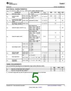
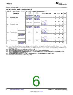
TCA9517
www.ti.com
SCPS242 –DECEMBER 2012
APPLICATION INFORMATION
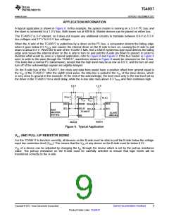
A typical application is shown in Figure 6. In this example, the system master is running on a 3.3-V I2C bus, and
the slave is connected to a 1.2-V bus. Both buses run at 400 kHz. Master devices can be placed on either bus.
The TCA9517 is 5-V tolerant, so it does not require any additional circuitry to translate between 0.9-V to 5.5-V
bus voltages and 2.7-V to 5.5-V bus voltages.
When the A side of the TCA9517 is pulled low by a driver on the I2C bus, a comparator detects the falling edge
when it goes below 0.3 VCCA and causes the internal driver on the B side to turn on, causing the B side to pull
down to about 0.5 V. When the B side of the TCA9517 falls, first a CMOS hysteresis-type input detects the falling
edge and causes the internal driver on the A side to turn on and pull the A-side pin down to ground. In order to
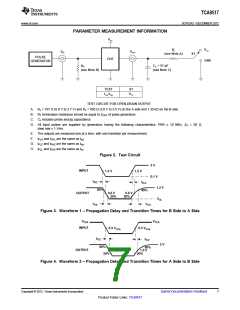
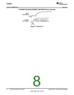
illustrate what would be seen in a typical application, refer to Figure 8 and Figure 9. If the bus master in Figure 6
were to write to the slave through the TCA9517, waveforms shown in Figure 8 would be observed on the A bus.
This looks like a normal I2C transmission, except that the high level may be as low as 0.9 V, and the turn on and
turn off of the acknowledge signals are slightly delayed.
On the B-side bus of the TCA9517, the clock and data lines would have a positive offset from ground equal to
the VOL of the TCA9517. After the eighth clock pulse, the data line is pulled to the VOL of the slave device, which
is very close to ground in this example. At the end of the acknowledge, the level rises only to the low level set by
the driver in the TCA9517 for a short delay, while the A-bus side rises above 0.3 VCCA and then continues high.
3.3 V
1.2 V
10 kW
VCCA
10 kW
10 kW
VCCB
10 kW
SDA
SCL
SDA
SCL
SDAB
SDAA
SCLB
SCLA
BUS
TCA9517
EN
MASTER
400 kHz
SLAVE
400 kHz
BUS A
BUS B
Figure 6. Typical Application
VILC AND PULL-UP RESISTOR SIZING
For the TCA9517 to function correctly, all devices on the B-side must be able to pull the B-side below the voltage
input low contention level (VILC). This means that the VOL of any device on the B-side must be below 0.4V.
VOL of a device can be adjusted by changing the IOL through the device which is set by the pull-up resistance
value. The pull-up resistance on the B-side must be carefully selected to ensure that logic levels will be
transferred correctly to the A-side.
Copyright © 2012, Texas Instruments Incorporated
Submit Documentation Feedback
9
Product Folder Links: TCA9517

 TI [ TEXAS INSTRUMENTS ]