TAS5707
www.ti.com ........................................................................................................................................................................................... SLOS556–NOVEMBER 2008
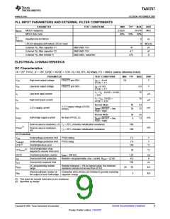
PLL INPUT PARAMETERS AND EXTERNAL FILTER COMPONENTS
PARAMETER
MCLK Frequency
TEST CONDITIONS
MIN
2.8224
40%
TYP
MAX
24.576
60%
UNIT
fMCLKI
MHz
MCLK duty cycle
50%
tr /
tf(MCLK)
Rise/fall time for MCLK
5
4
ns
LRCLK allowable drift before LRCLK reset
External PLL filter capacitor C1
External PLL filter capacitor C2
External PLL filter resistor R
MCLKs
nF
SMD 0603 Y5V
47
4.7
SMD 0603 Y5V
nF
SMD 0603, metal film
470
Ω
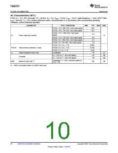
ELECTRICAL CHARACTERISTICS
DC Characteristics
TA = 25°, PVCC_X = 18V, DVDD = AVDD = 3.3V, RL= 8Ω, BTL AD Mode, FS = 48KHz (unless otherwise noted)
PARAMETER
High-level output voltage
TEST CONDITIONS
MIN TYP
MAX
UNIT
VOH
VOL
FAULTZ and SDA
FAULTZ and SDA
IOH = –4 mA
DVDD = 3 V
2.4
V
Low-level output voltage
IOL = 4 mA
DVDD = 3 V
0.5
75
75
V
VI < VIL ; DVDD = AVDD
= 3.6V
IIL
Low-level input current
High-level input current
µA
µA
VI > VIH ; DVDD =
AVDD = 3.6V
IIH
Normal Mode
48
24
83
32
3.3 V supply voltage (DVDD,
AVDD)
IDD
3.3 V supply current
mA
mA
mΩ
Reset (RESET = low,
PDN = high)
Normal Mode
30
5
55
13
IPVDD
Half-bridge supply current
No load (PVDD_X)
Reset (RESET = low,
PDN = high)
Drain-to-source resistance, LS TJ = 25°C, includes metallization resistance
180
180
(1)
rDS(on)
Drain-to-source resistance,
TJ = 25°C, includes metallization resistance
HS
I/O Protection
Vuvp
Undervoltage protection limit
PVDD falling
PVDD rising
7.2
7.6
V
V
Vuvp,hyst
OTE(2)
Undervoltage protection limit
Overtemperature error
150
°C
Extra temperature drop
required to recover from error
(2)
OTEHYST
30
°C
OLPC
IOC
Overload protection counter
Overcurrent limit protection
Overcurrent response time
fPWM = 384 kHz
1.25
4.5
ms
A
Resistor—programmable, max. current, ROCP = 22 kΩ
IOCT
150
ns
OC programming resistor
range
Resistor tolerance = 5% for typical value; the minimum
resistance should not be less than 20 kΩ.
ROCP
RPD
20
22
3
kΩ
kΩ
Internal pulldown resistor at
the output of each half-bridge capacitor charge.
Connected when drivers are tristated to provide bootstrap
(1) This does not include bond-wire or pin resistance.
(2) Specified by design
Copyright © 2008, Texas Instruments Incorporated
Submit Documentation Feedback
9
Product Folder Link(s): TAS5707

 TI [ TEXAS INSTRUMENTS ]