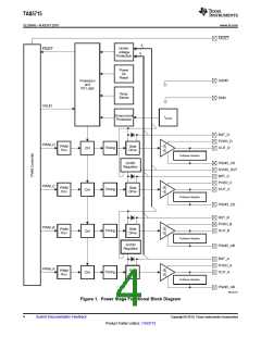
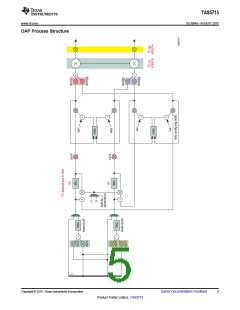
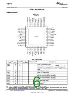
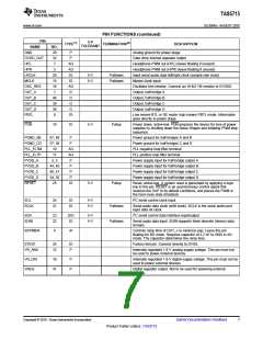
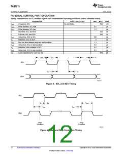
TAS5715
SLOS645 –AUGUST 2010
www.ti.com
ABSOLUTE MAXIMUM RATINGS
over operating free-air temperature range (unless otherwise noted)
(1)
VALUE
–0.3 to 3.6
–0.3 to 30
–0.5 to DVDD + 0.5
–0.5 to DVDD + 2.5(3)
–0.5 to AVDD + 2.5(3)
32(4)
UNIT
V
DVDD, AVDD
Supply voltage
PVDD_x
V
3.3-V digital input
V
Input voltage
5-V tolerant(2) digital input (except MCLK)
V
5-V tolerant MCLK input
V
OUT_x to PGND_x
BST_x to PGND_x
V
43(4)
V
Input clamp current, IIK
±20
mA
mA
°C
°C
°C
Output clamp current, IOK
±20
Operating free-air temperature
Operating junction temperature range
Storage temperature range, Tstg
0 to 85
0 to 150
–40 to 125
(1) Stresses beyond those listed under absolute ratings may cause permanent damage to the device. These are stress ratings only and
functional operation of the device at these or any other conditions beyond those indicated under recommended operation conditions are
not implied. Exposure to absolute-maximum conditions for extended periods may affect device reliability.
(2) 5-V tolerant inputs are PDN, RESET, SCLK, LRCLK, MCLK, SDIN, SDA, and SCL.
(3) Maximum pin voltage should not exceed 6.0V
(4) DC voltage + peak ac waveform measured at the pin should be below the allowed limit for all conditions.
DISSIPATION RATINGS(1)
DERATING FACTOR
ABOVE TA = 25°C
T
A ≤ 25°C
TA = 45°C
POWER RATING
TA = 70°C
POWER RATING
PACKAGE
POWER RATING
7-mm × 7-mm HTQFP
20 mW/°C
2 W
1.6 W
1.1 W
(1) This data was taken using 1 oz trace and copper pad that is soldered directly to a JEDEC standard high-k PCB. The thermal pad must
be soldered to a thermal land on the printed-circuit board. See TI Technical Briefs SLMA002 for more information about using the
HTQFP thermal pad
RECOMMENDED OPERATING CONDITIONS
MIN NOM
MAX
3.6
UNIT
V
Digital/analog supply voltage
Half-bridge supply voltage
High-level input voltage
DVDD, AVDD
PVDD_x
3
8
2
3.3
26
V
VIH
VIL
TA
5-V tolerant
5-V tolerant
V
Low-level input voltage
0.8
85
V
Operating ambient temperature range
Operating junction temperature range
Load impedance
0
0
°C
°C
Ω
(1)
TJ
125
RL (BTL)
Output filter: L = 15 mH, C = 680 nF.
4
8
Minimum output inductance under
short-circuit condition
10
LO (BTL)
Output-filter inductance
mH
(1) Continuous operation above the recommended junction temperature may result in reduced reliability and/or lifetime of the device.
PWM OPERATION AT RECOMMENDED OPERATING CONDITIONS
PARAMETER
TEST CONDITIONS
11.025/22.05/44.1-kHz data rate ±1%
48/24/12/8/16/32-kHz data rate ±1%
VALUE
352.8
384
UNIT
kHz
Output sample rate
8
Submit Documentation Feedback
Copyright © 2010, Texas Instruments Incorporated
Product Folder Link(s): TAS5715

 TI [ TEXAS INSTRUMENTS ]