TAS5715
SLOS645 –AUGUST 2010
www.ti.com
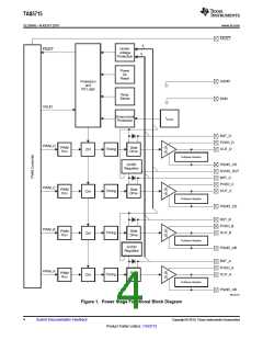
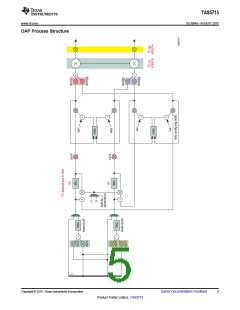
FAULT
4
Under-
voltage
Protection
FAULT
4
Power
On
Reset
AGND
GND
Protection
and
I/O Logic
Temp.
Sense
VALID
Overcurrent
Protection
Isense
BST_D
PVDD_D
OUT_D
PWM_D
PWM
Rcv
Gate
Drive
Timing
Timing
Timing
Timing
Ctrl
Ctrl
Ctrl
Ctrl
Pulldown Resistor
Pulldown Resistor
Pulldown Resistor
Pulldown Resistor
GVDD
Regulator
PGND_CD
GVDD_OUT
BST_C
PVDD_C
OUT_C
PWM_C
PWM_B
PWM_A
Gate
Drive
PWM
Rcv
PGND_CD
BST_B
PVDD_B
OUT_B
Gate
Drive
PWM
Rcv
GVDD
Regulator
PGND_AB
BST_A
PVDD_A
OUT_A
Gate
Drive
PWM
Rcv
PGND_AB
B0034-06
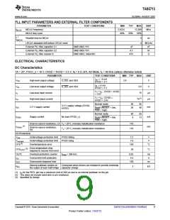
Figure 1. Power Stage Functional Block Diagram
4
Submit Documentation Feedback
Copyright © 2010, Texas Instruments Incorporated
Product Folder Link(s): TAS5715

 TI [ TEXAS INSTRUMENTS ]