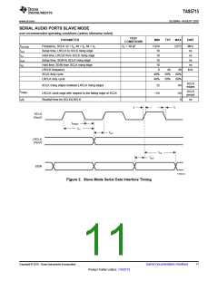
TAS5715
www.ti.com
SLOS645 –AUGUST 2010
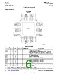
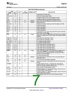
PIN FUNCTIONS (continued)
PIN
NAME
GND
5-V
TOLERANT
TYPE(1)
TERMINATION(2)
DESCRIPTION
NO.
29
32
7
P
P
Analog ground for power stage
Gate drive internal regulator output
GVDD_OUT
HPL
AO
AO
DI
DI
AO
O
Headphone PWM out (HPL) (leave floating if unused)
Headphone PWM out (HPR) (leave floating if unused)
Input serial audio data left/right clock (sample rate clock)
Master clock input
HPR
5
LRCLK
MCLK
20
15
16
1
5-V
5-V
Pulldown
Pulldown
OSC_RES
OUT_A
OUT_B
OUT_C
OUT_D
PBTL
Oscillator trim resistor. Connect an 18-kΩ 1% resistor to DVSSO.
Output, half-bridge A
46
39
36
8
O
Output, half-bridge B
O
Output, half-bridge C
O
Output, half-bridge D
DI
Low means BTL or SE mode; high means PBTL mode. Information
goes directly to power stage.
PDN
19
DI
5-V
Pullup
Power down, active-low. PDN prepares the device for loss of power
supplies by shutting down the Noise Shaper and initiating PWM stop
sequence.
PGND_AB
PGND_CD
PLL_FLTM
PLL_FLTP
PVDD_A
PVDD_B
PVDD_C
PVDD_D
RESET
47, 48
37, 38
10
P
P
Power ground for half-bridges A and B
Power ground for half-bridges C and D
PLL negative loop filter terminal
AO
AO
P
11
PLL positive loop filter terminal
2, 3
Power supply input for half-bridge output A
Power supply input for half-bridge output B
Power supply input for half-bridge output C
Power supply input for half-bridge output D
44, 45
40, 41
34, 35
25
P
P
P
DI
5-V
Pullup
Reset, active-low. A system reset is generated by applying a logic
low to this pin. RESET is an asynchronous control signal that
restores the DAP to its default conditions, and places the PWM in
the hard mute state (tristated).
SCL
24
21
DI
DI
5-V
5-V
I2C serial control clock input
SCLK
Pulldown
Pulldown
Serial audio data clock (shift clock). SCLK is the serial audio port
input data bit clock.
I2C serial control data interface input/output
SDA
23
22
DIO
DI
5-V
5-V
SDIN
Serial audio data input. SDIN supports three discrete (stereo) data
formats.
SSTIMER
6
AI
Controls ramp time of OUT_x to minimize pop. Leave this pin
floating for BD mode. Requires capacitor of 2.2 nF to GND in AD
mode. The capacitor determines the ramp time.
STEST
26
12
DI
P
Factory test pin. Connect directly to DVSS.
VR_ANA
Internally regulated 1.8-V analog supply voltage. This pin must not
be used to power external devices.
VR_DIG
VREG
18
31
P
P
Internally regulated 1.8-V digital supply voltage. This pin must not be
used to power external devices.
Digital regulator output. Not to be used for powering external
circuitry.
Copyright © 2010, Texas Instruments Incorporated
Submit Documentation Feedback
7
Product Folder Link(s): TAS5715

 TI [ TEXAS INSTRUMENTS ]