TAS5715
SLOS645 –AUGUST 2010
www.ti.com
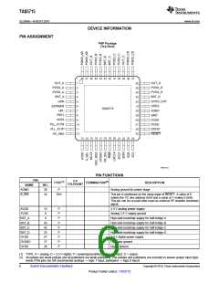
DEVICE INFORMATION
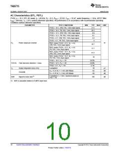
PIN ASSIGNMENT
PHP Package
(Top View)
48 47 46 45 44 43 42 41 40 39 38 37
OUT_A
OUT_D
PVDD_D
PVDD_D
BST_D
GVDD_OUT
VREG
1
36
35
34
33
32
31
30
29
28
27
26
25
PVDD_A
PVDD_A
BST_A
2
3
4
HPR
SSTIMER
HPL
5
6
TAS5715
7
AGND
PBTL
8
GND
AVSS
9
DVSS
PLL_FLTM
10
11
12
DVDD
PLL_FLTP
VR_ANA
STEST
RESET
13 14 15 16 17 18 19 20 21 22 23 24
P0075-10
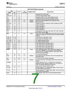
PIN FUNCTIONS
PIN
NAME
AGND
5-V
TOLERANT
TYPE(1)
TERMINATION(2)
DESCRIPTION
NO.
30
P
Analog ground for power stage
A_SEL
14
DIO
This pin is monitored on the rising edge of RESET. A value of 0
makes the I2C dev address 0x54 and a value of 1 makes it 0x56.
This pin can be re-used after reset as external HP amplifer shutdown
signal.
AVDD
AVSS
13
9
P
P
P
P
P
P
P
P
P
3.3-V analog power supply
Analog 3.3-V supply ground
BST_A
BST_B
BST_C
BST_D
DVDD
DVSSO
DVSS
4
High-side bootstrap supply for half-bridge A
High-side bootstrap supply for half-bridge B
High-side bootstrap supply for half-bridge C
High-side bootstrap supply for half-bridge D
3.3-V digital power supply
43
42
33
27
17
28
Oscillator ground
Digital ground
(1) TYPE: A = analog; D = 3.3-V digital; P = power/ground/decoupling; I = input; O = output
(2) All pullups are weak pullups and all pulldowns are weak pulldowns. The pullups and pulldowns are included to assure proper input logic
levels if the pins are left unconnected (pullups → logic 1 input; pulldowns → logic 0 input).
6
Submit Documentation Feedback
Copyright © 2010, Texas Instruments Incorporated
Product Folder Link(s): TAS5715

 TI [ TEXAS INSTRUMENTS ]