SN54LVTH16373, SN74LVTH16373
3.3-V ABT 16-BIT TRANSPARENT D-TYPE LATCHES
WITH 3-STATE OUTPUTS
www.ti.com
SCBS144P–MAY 1992–REVISED NOVEMBER 2006
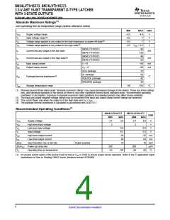
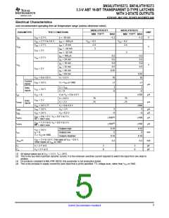
Absolute Maximum Ratings(1)
over operating free-air temperature range (unless otherwise noted)
MIN
–0.5
–0.5
–0.5
MAX
4.6
UNIT
VCC
VI
Supply voltage range
Input voltage range(2)
Voltage range applied to any output in the high-impedance or power-off state(2)
Voltage range applied to any output in the high state(2)
V
7
7
V
V
V
VO
VO
–0.5 VCC + 0.5
SN54LVTH16373
Current into any output in the low state
96
128
48
IO
mA
mA
SN74LVTH16373
SN54LVTH16373
Current into any output in the high state(3)
SN74LVTH16373
IO
64
IIK
Input clamp current
Output clamp current
VI < 0
–50
–50
70
mA
mA
IOK
VO < 0
DGG package
DL package
GQL/ZQL package
GRD/ZRD package
63
θJA
Package thermal impedance(4)
°C
°C
42
36
Tstg
Storage temperature range
–65
150
(1) Stresses beyond those listed under "absolute maximum ratings" may cause permanent damage to the device. These are stress ratings
only, and functional operation of the device at these or any other conditions beyond those indicated under "recommended operating
conditions" is not implied. Exposure to absolute-maximum-rated conditions for extended periods may affect device reliability.
(2) The input and output negative-voltage ratings may be exceeded if the input and output clamp-current ratings are observed.
(3) This current flows only when the output is in the high state and VO > VCC
.
(4) The package thermal impedance is calculated in accordance with JESD 51-7.
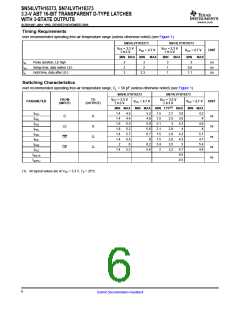
Recommended Operating Conditions(1)
SN54LVTH16373
SN74LVTH16373
UNIT
MIN
2.7
2
MAX
MIN
2.7
2
MAX
VCC
VIH
Supply voltage
3.6
3.6
V
V
High-level input voltage
Low-level input voltage
Input voltage
VIL
0.8
5.5
–24
48
0.8
5.5
–32
64
V
VI
V
IOH
High-level output current
Low-level output current
Input transition rise or fall rate
Power-up ramp rate
mA
mA
IOL
∆t/∆v
∆t/∆VCC
TA
Outpts enabled
10
10 ns/V
200
–55
200
–40
µs/V
Operating free-air temperature
125
85
°C
(1) All unused control inputs of the device must be held at VCC or GND to ensure proper device operation. Refer to the TI application report,
Implications of Slow or Floating CMOS Inputs, literature number SCBA004.
4
Submit Documentation Feedback

 TI [ TEXAS INSTRUMENTS ]