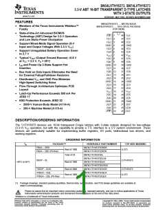
SN54LVTH16373, SN74LVTH16373
3.3-V ABT 16-BIT TRANSPARENT D-TYPE LATCHES
WITH 3-STATE OUTPUTS
www.ti.com
SCBS144P–MAY 1992–REVISED NOVEMBER 2006
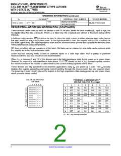
ORDERING INFORMATION (continued)
TA
PACKAGE(1)
ORDERABLE PART NUMBER
SNJ54LVTH16373WD
5962-9681001QXA
TOP-SIDE MARKING
Tube
–55°C to 125°C
CFP – WD
SNJ54LVTH16373WD
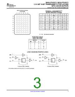
DESCRIPTION/ORDERING INFORMATION (CONTINUED)
These devices can be used as two 8-bit latches or one 16-bit latch. When the latch-enable (LE) input is high, the
Q outputs follow the data (D) inputs. When LE is taken low, the Q outputs are latched at the levels set up at the
D inputs.
A buffered output-enable (OE) input can be used to place the eight outputs in either a normal logic state (high or
low logic levels) or a high-impedance state. In the high-impedance state, the outputs neither load nor drive the
bus lines significantly. The high-impedance state and the increased drive provide the capability to drive bus lines
without interface or pullup components.
OE does not affect internal operations of the latch. Old data can be retained or new data can be entered while
the outputs are in the high-impedance state.
Active bus-hold circuitry holds unused or undriven inputs at a valid logic state. Use of pullup or pulldown
resistors with the bus-hold circuitry is not recommended.
When VCC is between 0 and 1.5 V, the devices are in the high-impedance state during power up or power down.
However, to ensure the high-impedance state above 1.5 V, OE should be tied to VCC through a pullup resistor;
the minimum value of the resistor is determined by the current-sinking capability of the driver.
These devices are fully specified for hot-insertion applications using Ioff and power-up 3-state. The Ioff circuitry
disables the outputs, preventing damaging current backflow through the devices when they are powered down.
The power-up 3-state circuitry places the outputs in the high-impedance state during power up and power down,
which prevents driver conflict.
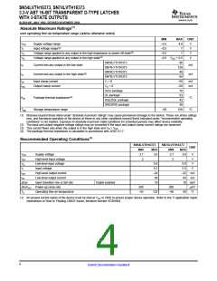
TERMINAL ASSIGNMENTS(1)
(56-Ball GQL/ZQL Package)
GQL OR ZQL PACKAGE
(TOP VIEW)
1
2 3 4 5 6
1
2
3
4
5
6
A
B
C
D
E
F
1OE
1Q2
1Q4
1Q6
1Q8
2Q1
2Q3
2Q5
2Q7
2OE
NC
NC
NC
NC
1CLK
1D2
1D4
1D6
1D8
2D1
2D3
2D5
2D7
2CLK
A
B
C
D
E
F
G
H
J
1Q1
1Q3
1Q5
1Q7
2Q2
2Q4
2Q6
2Q8
NC
GND
VCC
GND
GND
VCC
GND
1D1
1D3
1D5
1D7
2D2
2D4
2D6
2D8
NC
G
H
J
GND
VCC
GND
NC
GND
VCC
GND
NC
K
K
(1) NC – No internal connection
2
Submit Documentation Feedback

 TI [ TEXAS INSTRUMENTS ]