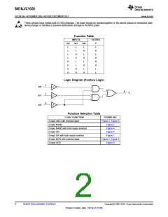
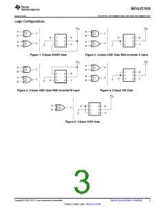
SN74LVC1G58
SCES415N –NOVEMBER 2002–REVISED DECEMBER 2013
www.ti.com
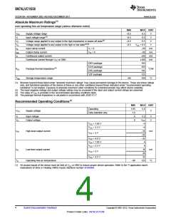
Absolute Maximum Ratings(1)
over operating free-air temperature range (unless otherwise noted)
MIN
–0.5
–0.5
–0.5
–0.5
MAX UNIT
VCC
VI
Supply voltage range
Input voltage range(2)
Voltage range applied to any output in the high-impedance or power-off state(2)
Voltage range applied to any output in the high or low state(2)(3)
6.5
6.5
V
V
VO
VO
IIK
6.5
V
VCC + 0.5
–50
V
Input clamp current
VI < 0
mA
mA
mA
mA
IOK
IO
Output clamp current
VO < 0
–50
Continuous output current
Continuous current through VCC or GND
±50
±100
165
DBV package
DCK package
DRL package
YZP package
259
θJA
Package thermal impedance(4)
°C/W
°C
142
123
Tstg
Storage temperature range
–65
150
(1) Stresses beyond those listed under "absolute maximum ratings" may cause permanent damage to the device. These are stress ratings
only, and functional operation of the device at these or any other conditions beyond those indicated under "recommended operating
conditions" is not implied. Exposure to absolute-maximum-rated conditions for extended periods may affect device reliability.
(2) The input negative-voltage and output voltage ratings may be exceeded if the input and output current ratings are observed.
(3) The value of VCC is provided in the recommended operating conditions table.
(4) The package thermal impedance is calculated in accordance with JESD 51-7.
Recommended Operating Conditions(1)
MIN
1.65
1.5
0
MAX UNIT
Operating
5.5
V
VCC
Supply voltage
Data retention only
VI
Input voltage
5.5
VCC
–4
V
V
VO
Output voltage
0
VCC = 1.65 V
VCC = 2.3 V
–8
IOH
High-level output current
–16
–24
–32
4
mA
VCC = 3 V
VCC = 4.5 V
VCC = 1.65 V
VCC = 2.3 V
8
IOL
Low-level output current
16
mA
°C
VCC = 3 V
24
VCC = 4.5 V
32
TA
Operating free-air temperature
–40
125
(1) All unused inputs of the device must be held at VCC or GND to ensure proper device operation. Refer to the TI application report,
Implications of Slow or Floating CMOS Inputs, literature number SCBA004.
4
Submit Documentation Feedback
Copyright © 2002–2013, Texas Instruments Incorporated
Product Folder Links: SN74LVC1G58

 TI [ TEXAS INSTRUMENTS ]