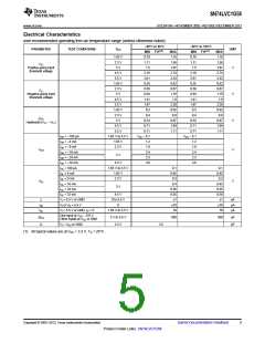
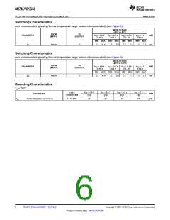
SN74LVC1G58
www.ti.com
SCES415N –NOVEMBER 2002–REVISED DECEMBER 2013
Configurable Multiple-Function Gate
Check for Samples: SN74LVC1G58
1
FEATURES
DESCRIPTION
This configurable multiple-function gate is designed
for 1.65-V to 5.5-V VCC operation.
2
•
Available in the Texas Instruments NanoFree™
Package
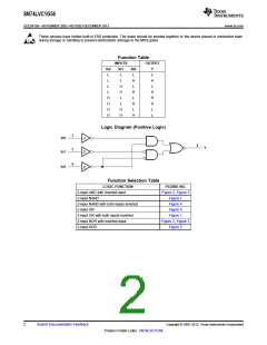
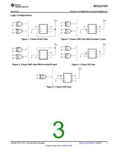
The SN74LVC1G58 device features configurable
multiple functions. The output state is determined by
eight patterns of 3-bit input. The user can choose the
logic functions AND, OR, NAND, NOR, XOR, inverter,
and noninverter. All inputs can be connected to VCC
or GND.
•
•
•
•
•
•
•
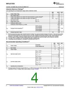
Supports 5-V VCC Operation
Inputs Accept Voltages to 5.5 V
Supports Down Translation to VCC
Max tpd of 6.3 ns at 3.3 V
Low Power Consumption, 10-µA Max ICC
±24-mA Output Drive at 3.3 V
This device functions as an independent gate, but
because of Schmitt action, it may have different input
threshold levels for positive-going (VT+) and negative-
going (VT–) signals.
Ioff Supports Live Insertion, Partial-Power-
Down Mode, and Back-Drive Protection
•
•
Latch-Up Performance Exceeds 100 mA Per
JESD 78, Class II
NanoFree™ package technology is
a
major
breakthrough in IC packaging concepts, using the die
as the package.
ESD Protection Exceeds JESD 22
–
–
–
2000-V Human-Body Model (A114-A)
200-V Machine Model (A115-A)
This device is fully specified for partial-power-down
applications using Ioff. The Ioff circuitry disables the
outputs, preventing damaging current backflow
through the device when it is powered down.
1000-V Charged-Device Model (C101)
DBV PACKAGE
(TOP VIEW)
DCK PACKAGE
(TOP VIEW)
DRL PACKAGE
(TOP VIEW)
YZP PACKAGE
(BOTTOM VIEW)
3
4
Y
V
In0
GND
In1
1
2
3
6
In1
GND
In0
In2
V
In1
GND
In0
In2
V
1
2
3
6
1
2
3
6
In1
GND
In0
In2
V
2 5
CC
5
4
CC
5
4
CC
1
6
In2
Y
CC
5
4
Y
Y
DRY PACKAGE
(TOP VIEW)
DSF PACKAGE
(TOP VIEW)
1
2
3
6
5
4
ln2
ln1
GND
ln0
1
2
3
6
5
4
ln1
ln2
VCC
Y
VCC
Y
See mechanical drawings for dimensions.
GND
ln0
1
Please be aware that an important notice concerning availability, standard warranty, and use in critical applications of
Texas Instruments semiconductor products and disclaimers thereto appears at the end of this data sheet.
2
NanoFree is a trademark of Texas Instruments.
PRODUCTION DATA information is current as of publication date.
Products conform to specifications per the terms of the Texas
Instruments standard warranty. Production processing does not
necessarily include testing of all parameters.
Copyright © 2002–2013, Texas Instruments Incorporated

 TI [ TEXAS INSTRUMENTS ]