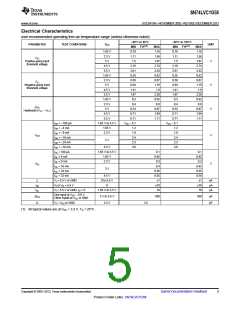
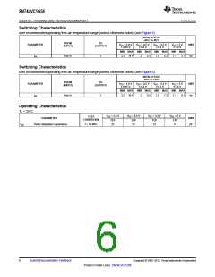
SN74LVC1G58
SCES415N –NOVEMBER 2002–REVISED DECEMBER 2013
www.ti.com
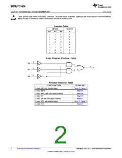
These devices have limited built-in ESD protection. The leads should be shorted together or the device placed in conductive foam
during storage or handling to prevent electrostatic damage to the MOS gates.
Function Table
INPUTS
OUTPUT
In2
L
In1
L
In0
L
Y
L
L
L
H
L
H
L
L
H
H
L
L
H
L
H
H
H
L
H
H
H
H
L
H
L
H
H
H
L
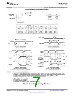
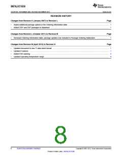
Logic Diagram (Positive Logic)
3
1
In0
In1
4
Y
6
In2
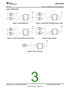
Function Selection Table
LOGIC FUNCTION
FIGURE NO.
2-input AND with inverted input
2-input NAND
Figure 2, Figure 3
Figure 1
2-input NAND with both inputs inverted
2-input OR
Figure 4
Figure 4
2-input OR with both inputs inverted
2-input NOR with inverted input
2-input XOR
Figure 1
Figure 2, Figure 3
Figure 5
2
Submit Documentation Feedback
Copyright © 2002–2013, Texas Instruments Incorporated
Product Folder Links: SN74LVC1G58

 TI [ TEXAS INSTRUMENTS ]