SN65HVS883
www.ti.com.cn
ZHCSFI0 –SEPTEMBER 2016
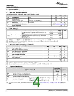
6.5 Electrical Characteristics
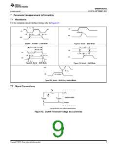
all voltages measured against FGND unless otherwise stated, see Figure 12
SYMBOL
VTH–(IP)
VTH+(IP)
VHYS(IP)
VTH–(IN)
VTH+(IN)
VHYS(IN)
PARAMETER
Low-level device input threshold voltage
High-level device input threshold voltage
Device input hysteresis
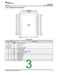
PIN
TEST CONDITIONS
MIN
TYP
4.3
5.2
0.9
8.4
9.4
1
MAX UNIT
4
V
18 V< V24 < 34 V,
RIN = 0 Ω ,
RLIM = 25 kΩ
5.5
10
V
V
V
V
V
V
V
V
IP0–IP7
Low-level field input threshold voltage
High-level field input threshold voltage
Field input hysteresis
6
18 V < V24 < 34 V,
RIN = 1.2 kΩ ± 5%,
RLIM = 25 kΩ
measured at
field side of RIN
VTH–(V24) Low-level V24-monitor threshold voltage
VTH+(V24) High-level V24-monitor threshold voltage
VHYS(V24) V24-monitor hysteresis
15 16.05
16.8
V24
18
0.75
3 V < VIPx < 6 V,
RIN = 1.2 kΩ ± 5%,
RLIM = 25 kΩ
RIP
Input resistance
1.4
1.83
3.6
2.3
kΩ
IP0–IP7
10 V < VIPx < 34 V,
RLIM = 25 kΩ
IIP-LIM
Input current limit
3.15
4
mA
VOL
VOH
Logic low-level output voltage
Logic high-level output voltage
IOL = 20 μA
0.4
V
V
SOP, CHOK
IOH = –20 μA
4
DB0, DB1, SIP,
LD, CE, CLK
IIL
Logic input leakage current
RE on-state current
–50
50
μA
RLIM = 25 kΩ,
REX = FGND
IRE-on
RE0–RE7
2.8
3.15
3.5
mA
IP0 to IP7 = V24,
5VOP = open,
REX = FGND,
ICC(V24)
Supply current
V24
8.7
mA
V
All logic inputs open
18 V < V24 < 34 V,
no load
4.5
4.5
5
5.5
5.5
VO(5V)
Linear regulator output voltage
5VOP
18 V < V24 < 34 V,
IL = 50 mA
5
ILIM(5V)
Linear regulator output current limit
115
mA
18 V < V24 < 34 V,
IL = 5 mA
ΔV5/ΔV24 Line regulation
5VOP, V24
IP0–IP7
2
mV/V
DB0 = open,
DB1 = FGND
0
tDB
Debounce times of input channels
DB0 = FGND,
DB1 = open
ms
ms
1
3
1
DB0 = DB1 = open
Voltage monitor debounce time after V24 < 15
V (CHOK turns low)
tDB-HL
V24, CHOK
Voltage monitor debounce time after V24 > 18
V (CHOK turns high)
tDB-LH
TSHDN
6
ms
°C
Shutdown temperature
170
Copyright © 2016, Texas Instruments Incorporated
5

 TI [ TEXAS INSTRUMENTS ]