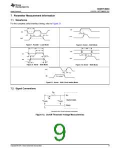
SN65HVS883
ZHCSFI0 –SEPTEMBER 2016
www.ti.com.cn
6 Specifications
6.1 Absolute Maximum Ratings
over operating free-air temperature range (unless otherwise noted)
MIN
–0.3
–0.3
–0.5
MAX
UNIT
V
V24
VIPx
VID
IO
Field power input
V24
36
36
6
Field digital inputs
IPx
V
Voltage at any logic input
Output current
DB0, DB1, CLK, SIP, CE, LD
CHOK, SOP
V
±8
mA
PTOT
TJ
Continuous total power dissipation
Junction temperature
See Thermal Information table
170
°C
6.2 ESD Ratings
VALUE
±4000
UNIT
All pins
IPx,V24
Human-body model (HBM), per ANSI/ESDA/JEDEC JS-
001(1)
±15000
V(ESD)
Electrostatic discharge
V
Charged-device model (CDM), per JEDEC specification
JESD22-C101(2)
Machine Mode(3)
All pins
All pins
±1000
±100
(1) JEDEC document JEP155 states that 500-V HBM allows safe manufacturing with a standard ESD control process.
(2) JEDEC document JEP157 states that 250-V CDM allows safe manufacturing with a standard ESD control process.
(3) JEDEC Standard 22, Method A115-A.
6.3 Recommended Operating Conditions
MIN
10
0
TYP
MAX
34
UNIT
V24
VIPL
VIPH
VIL
Field supply voltage
24
V
V
Field input low-state input voltage(1)
Field input high-state input voltage(1)
Logic low-state input voltage
Logic high-state input voltage
Current limiter resistor
4
10
0
34
V
0.8
5.5
500
1
V
VIH
RLIM
fIP
2
V
17
0
25
kΩ
Mbps
°C
°C
Input data rate(2)
TJ
150
85
TA
–40
(1) Field input voltages correspond to an input resistor of RIN = 1.2 kΩ
(2) Maximum data rate corresponds to 0 ms debounce time, (DB0 = open, DB1 = FGND), and RIN = 0 Ω
6.4 Thermal Information
SN65HVS883
THERMAL METRIC(1)
PWP (HTSSOP)
UNIT
28 PINS
35
RθJA
Junction-to-ambient thermal resistance
Junction-to-case (top) thermal resistance
Junction-to-board thermal resistance
°C/W
°C/W
°C/W
RθJC(top)
RθJB
4.27
15
ILOAD = 50 mA, RIN = 0, IPO–IP7 = V24 = 30 V,
PD
Device power dissipation
RE7 = FGND, fCLK = 100 MHz,
2591
mW
IIP-LIM and ICC = worst case with RLIM = 25 kΩ
(1) For more information about traditional and new thermal metrics, see the Semiconductor and IC Package Thermal Metrics application
report.
4
Copyright © 2016, Texas Instruments Incorporated

 TI [ TEXAS INSTRUMENTS ]