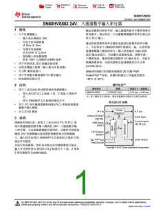
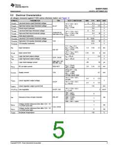
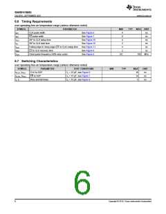
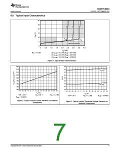
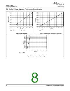
SN65HVS883
www.ti.com.cn
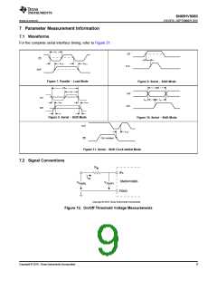
ZHCSFI0 –SEPTEMBER 2016
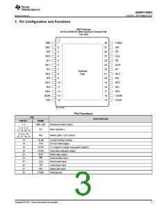
5 Pin Configuration and Functions
PWP Package
28 Pin (HTSSOP) With Exposed Thermal Pad
Top View
DB0
DB1
IP0
1
28
27
26
25
24
23
FGND
SIP
2
3
LD
RE0
IP1
4
CLK
CE
5
RE1
IP2
6
SOP
IP7
7
22
Thermal
Pad
RE2
IP3
8
21
20
19
18
17
16
15
RE7
IP6
9
RE3
IP4
10
11
12
13
14
RE6
IP5
RE4
RLIM
V24
RE5
CHOK
5VOP
Not to scale
Pin Functions
PIN
DESCRIPTION
PIN NO.
1, 2
NAME
DB0, DB1
Debounce select inputs
Input channel x
3, 5, 7, 9,
11, 18, 20, 22
IPx
4, 6, 8, 10,
12, 17, 19, 21
REx
Return path x (LED drive)
13
14
15
16
23
24
25
26
27
28
RLIM
V24
Current limiting resistor
24 VDC field supply
5VOP
CHOK
SOP
CE
5 V output to supply low-power isolators
Chip okay indicator output
Serial data output
Clock enable input
CLK
LD
Serial clock input
Load pulse input
SIP
Serial data input
FGND
Field ground
Copyright © 2016, Texas Instruments Incorporated
3

 TI [ TEXAS INSTRUMENTS ]