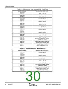
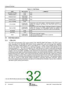
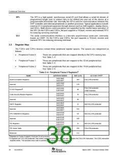
Functional Overview
3.2.6 Flash (F281x Only)
The F2812 and F2811 contain 128K x 16 of embedded flash memory, segregated into four 8K X 16 sectors,
and six 16K X 16 sectors. The F2810 has 64K X 16 of embedded flash, segregated into two 8K X 16 sectors,
and three 16K X 16 sectors. All three devices also contain a single 1K x 16 of OTP memory at address range
0x3D 7800 − 0x3D 7BFF. The user can indiviually erase, program, and validate a flash sector while leaving
other sectors untouched. However, it is not possible to use one sector of the flash or the OTP to execute flash
algorithms that erase/program other sectors. Special memory pipelining is provided to enable the flash module
to achieve higher performance. The flash/OTP is mapped to both program and data space; therefore, it can
be used to execute code or store data information.
NOTE:
The F2810/F2811/F2812 Flash and OTP wait states can be configured by the application. This
allows applications running at slower frequencies to configure the flash to use fewer
wait states.
Flash effective performance can be improved by enabling the flash pipeline mode in the Flash
options register. With this mode enabled, effective performance of linear code execution will
be much faster than the raw performance indicated by the wait state configuration alone. The
exact performance gain when using the Flash pipeline mode is application-dependent. The
pipeline mode is not available for the OTP block.
For more information on the Flash options, Flash wait-state, and OTP wait-state registers, see
the TMS320F28x System Control and Interrupts Reference Guide (literature number
SPRU078).
3.2.7 ROM (C281x Only)
The C2812 and C2811 contain 128K x 16 of ROM. The C2810 has 64K x 16 of ROM. In addition to this, there
is a 1K X 16 ROM block that replaces the OTP memory available in flash devices. For information on how to
submit ROM codes to TI, see the TMS320C28x CPU and Instruction Set Reference Guide (literature number
SPRU430).
3.2.8 M0, M1 SARAMs
All C28x devices contain these two blocks of single access memory, each 1K x 16 in size. The stack pointer
points to the beginning of block M1 on reset. The M0 block overlaps the 240x device B0, B1, B2 RAM blocks
and hence the mapping of data variables on the 240x devices can remain at the same physical address on
C28x devices. The M0 and M1 blocks, like all other memory blocks on C28x devices, are mapped to both
program and data space. Hence, the user can use M0 and M1 to execute code or for data variables. The
partitioning is performed within the linker. The C28x device presents a unified memory map to the programmer.
This makes for easier programming in high-level languages.
3.2.9 L0, L1, H0 SARAMs
The F281x and C281x contain an additional 16K x 16 of single-access RAM, divided into 3 blocks
(4K + 4K + 8K). Each block can be independently accessed hence minimizing pipeline stalls. Each block is
mapped to both program and data space.
3.2.10 Boot ROM
The Boot ROM is factory-programmed with boot-loading software. Boot-mode signals are provided to tell the
bootloader software what boot mode to use on power up. The user can select to boot normally or to download
new software from an external connection or to select boot software that is programmed in the internal Flash.
The Boot ROM will also contain standard tables, such as SIN/COS waveforms, for use in math related
algorithms.
34
SGUS051A
March 2004 − Revised October 2004

 TI [ TEXAS INSTRUMENTS ]