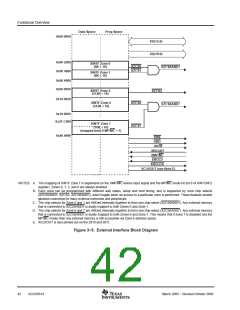
Functional Overview
SPI:
The SPI is a high-speed, synchronous serial I/O port that allows a serial bit stream of
programmed length (one to sixteen bits) to be shifted into and out of the device at a
programmable bit-transfer rate. Normally, the SPI is used for communications between the
DSP controller and external peripherals or another processor. Typical applications include
external I/O or peripheral expansion through devices such as shift registers, display drivers,
and ADCs. Multi-device communications are supported by the master/slave operation of
the SPI. On the F281x and C281x, the port supports a 16-level, receive and transmit FIFO
for reducing servicing overhead.
SCI:
The serial communications interface is a two-wire asynchronous serial port, commonly
known as UART. On the F281x and C281x, the port supports a 16-level, receive and
transmit FIFO for reducing servicing overhead.
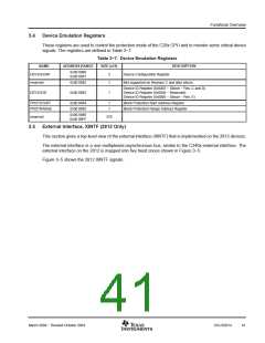
3.3
Register Map
The F281x and C281x devices contain three peripheral register spaces. The spaces are categorized as
follows:
•
•
•
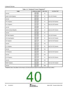
Peripheral Frame 0:
Peripheral Frame 1:
Peripheral Frame 2:
These are peripherals that are mapped directly to the CPU memory bus.
See Table 3−4.
These are peripherals that are mapped to the 32-bit peripheral bus.
See Table 3−5.
These are peripherals that are mapped to the 16-bit peripheral bus.
See Table 3−6.
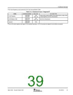
†
Table 3−4. Peripheral Frame 0 Registers
‡
NAME
ADDRESS RANGE
SIZE (x16)
ACCESS TYPE
0x00 0880
0x00 09FF
Device Emulation Registers
reserved
384
EALLOW protected
0x00 0A00
0x00 0A7F
128
96
EALLOW protected
CSM Protected
0x00 0A80
0x00 0ADF
§
FLASH Registers
0x00 0AE0
0x00 0AEF
Code Security Module Registers
reserved
16
48
EALLOW protected
0x00 0AF0
0x00 0B1F
0x00 0B20
0x00 0B3F
XINTF Registers
reserved
32
Not EALLOW protected
Not EALLOW protected
0x00 0B40
0x00 0BFF
192
64
0x00 0C00
0x00 0C3F
CPU-TIMER0/1/2 Registers
reserved
0x00 0C40
0x00 0CDF
160
32
0x00 0CE0
0x00 0CFF
PIE Registers
Not EALLOW protected
EALLOW protected
0x00 0D00
0x00 0DFF
PIE Vector Table
Reserved
256
512
0x00 0E00
0x00 0FFF
†
‡
Registers in Frame 0 support 16-bit and 32-bit accesses.
If registers are EALLOW protected, then writes cannot be performed until the user executes the EALLOW instruction. The EDIS instruction
disables writes. This prevents stray code or pointers from corrupting register contents.
38
SGUS051A
March 2004 − Revised October 2004

 TI [ TEXAS INSTRUMENTS ]