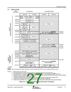
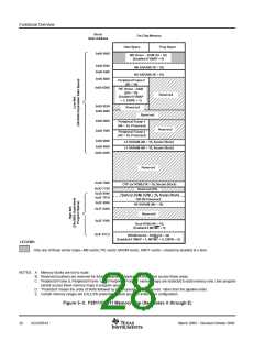
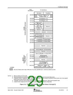
Functional Overview
The “Low 64K” of the memory address range maps into the data space of the 240x. The “High 64K” of the
memory address range maps into the program space of the 24x/240x. 24x/240x-compatible code will only
execute from the “High 64K” memory area. Hence, the top 32K of Flash/ROM and H0 SARAM block can be
used to run 24x/240x-compatible code (if MP/MC mode is low) or, on the 2812, code can be executed from
XINTF Zone 7 (if MP/MC mode is high).
The XINTF consists of five independent zones. One zone has its own chip select and the remaining four zones
share two chip selects. Each zone can be programmed with its own timing (wait states) and to either sample
or ignore external ready signal. This makes interfacing to external peripherals easy and glueless.
NOTE:
The chip selects of XINTF Zone 0 and Zone 1 are merged together into a single chip select
(XZCS0AND1); and the chip selects of XINTF Zone 6 and Zone 7 are merged together into
a single chip select (XZCS6AND7). See Section 3.5, “External Interface, XINTF (2812 only)”,
for details.
Peripheral Frame 1, Peripheral Frame 2, and XINTF Zone 1 are grouped together so as to enable these blocks
to be “write/read peripheral block protected”. The “protected” mode ensures that all accesses to these blocks
happen as written. Because of the C28x pipeline, a write immediately followed by a read, to different memory
locations, will appear in reverse order on the memory bus of the CPU. This can cause problems in certain
peripheral applications where the user expected the write to occur first (as written). The C28x CPU supports
a block protection mode where a region of memory can be protected so as to make sure that operations occur
as written (the penalty is extra cycles are added to align the operations). This mode is programmable and by
default, it will protect the selected zones.
On the 2812, at reset, XINTF Zone 7 is accessed if the XMP/MC pin is pulled high. This signal selects
microprocessor or microcomputer mode of operation. In microprocessor mode, Zone 7 is mapped to high
memory such that the vector table is fetched externally. The Boot ROM is disabled in this mode. In
microcomputer mode, Zone 7 is disabled such that the vectors are fetched from Boot ROM. This allows the
user to either boot from on-chip memory or from off-chip memory. The state of the XMP/MC signal on reset
is stored in an MP/MC mode bit in the XINTCNF2 register. The user can change this mode in software and
hence control the mapping of Boot ROM and XINTF Zone 7. No other memory blocks are affected by
XMP/MC.
I/O space is not supported on the 2812 XINTF.
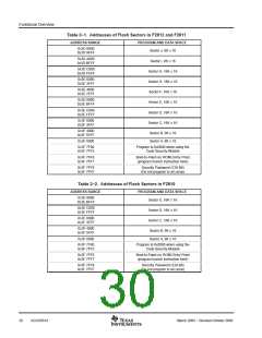
The wait states for the various spaces in the memory map area are listed in Table 3−3.
31
March 2004 − Revised October 2004
SGUS051A

 TI [ TEXAS INSTRUMENTS ]