Functional Overview
3.2.13 External Interrupts (XINT1, 2, 13, XNMI)
The F281x and C281x support three masked external interrupts (XINT1, 2, 13). XINT13 is combined with one
non-masked external interrupt (XNMI). The combined signal name is XNMI_XINT13. Each of the interrupts
can be selected for negative or positive edge triggering and can also be enabled/disabled (including the
XNMI). The masked interrupts also contain a 16-bit free running up counter, which is reset to zero when a valid
interrupt edge is detected. This counter can be used to accurately time stamp the interrupt.
3.2.14 Oscillator and PLL
The F281x and C281x can be clocked by an external oscillator or by a crystal attached to the on-chip oscillator
circuit. A PLL is provided supporting up to 10-input clock-scaling ratios. The PLL ratios can be changed
on-the-fly in software, enabling the user to scale back on operating frequency if lower power operation is
desired. Refer to the Electrical Specification section for timing details. The PLL block can be set in bypass
mode.
3.2.15 Watchdog
The F281x and C281x support a watchdog timer. The user software must regularly reset the watchdog counter
within a certain time frame; otherwise, the watchdog will generate a reset to the processor. The watchdog can
be disabled if necessary.
3.2.16 Peripheral Clocking
The clocks to each individual peripheral can be enabled/disabled so as to reduce power consumption when
a peripheral is not in use. Additionally, the system clock to the serial ports (except eCAN) and the event
managers, CAP and QEP blocks can be scaled relative to the CPU clock. This enables the timing of
peripherals to be decoupled from increasing CPU clock speeds.
3.2.17 Low-Power Modes
The F281x and C281x devices are full static CMOS devices. Three low-power modes are provided:
IDLE:
Place CPU into low-power mode. Peripheral clocks may be turned off selectively and only
those peripherals that need to function during IDLE are left operating. An enabled interrupt
from an active peripheral will wake the processor from IDLE mode.
STANDBY:
HALT:
Turn off clock to CPU and peripherals. This mode leaves the oscillator and PLL functional.
An external interrupt event will wake the processor and the peripherals. Execution begins
on the next valid cycle after detection of the interrupt event.
Turn off oscillator. This mode basically shuts down the device and places it in the lowest
possible power consumption mode. Only a reset or XNMI will wake the device from this
mode.
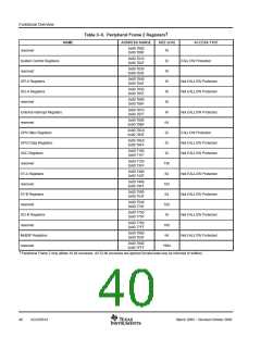
3.2.18 Peripheral Frames 0, 1, 2 (PFn)
The F281x and C281x segregate peripherals into three sections. The mapping of peripherals is as follows:
PF0:
XINTF:
PIE:
External Interface Configuration Registers (2812 only)
PIE Interrupt Enable and Control Registers Plus PIE Vector Table
Flash Control, Programming, Erase, Verify Registers
Flash:
Timers: CPU-Timers 0, 1, 2 Registers
CSM:
Code Security Module KEY Registers
eCAN Mailbox and Control Registers
PF1:
eCAN:
36
SGUS051A
March 2004 − Revised October 2004

 TI [ TEXAS INSTRUMENTS ]