RM48L950
RM48L750
RM48L550
SPNS174–SEPTEMBER 2011
www.ti.com
1
RM48Lx50 16/32-Bit RISC Flash Microcontroller
............................................................... 1
4.6 Clocks .............................................. 59
4.7 Clock Monitoring .................................... 67
1.1 Features .............................................. 1
1.2 Applications .......................................... 2
1.3 Description ........................................... 3
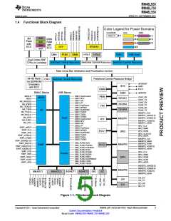
1.4 Functional Block Diagram ............................ 5
1.1 Device Configuration ................................. 7
Device Package and Terminal Functions ......... 10
4.8 Glitch Filters ........................................ 69
4.9 Device Memory Map ................................ 70
4.10 Flash Memory ...................................... 77
4.11 Tightly-Coupled RAM Interface Module ............ 80
4.12 Parity Protection for Accesses to peripheral RAMs
...................................................... 80
4.13 On-Chip SRAM Initialization and Testing ........... 82
4.14 External Memory Interface (EMIF) ................. 84
4.15 Vectored Interrupt Manager ........................ 91
4.16 DMA Controller ..................................... 94
4.17 Real Time Interrupt Module ........................ 97
4.18 Error Signaling Module ............................. 99
2
3
2.2 PGE QFP Package Pinout (144-Pin) ............... 10
2.3
ZWT BGA Package Ball-Map (337 Ball Grid Array)
...................................................... 11
2.4 Terminal Functions ................................. 12
Device Operating Conditions ....................... 44
3.1
Absolute Maximum Ratings Over Operating
4.19 Reset / Abort / Error Sources ..................... 103
Free-Air Temperature Range, ...................... 44
4.20 Digital Windowed Watchdog ...................... 105
4.21 Debug Subsystem ................................. 106
3.2
3.3
Device Recommended Operating Conditions ...... 44
Switching Characteristics over Recommended
5
Peripheral Information and Electrical
Operating Conditions for Clock Domains ........... 45
Specifications ......................................... 117
3.4 Wait States Required ............................... 45
3.5
5.1 Peripheral Legend ................................. 117
Power Consumption Over Recommended
5.2
Multi-Buffered 12bit Analog-to-Digital Converter
Operating Conditions ............................... 46
Input/Output Electrical Characteristics Over
..................................................... 117
3.6
5.3 General-Purpose Input/Output .................... 126
5.4 Enhanced High-End Timer (N2HET) .............. 127
5.5 Controller Area Network (DCAN) .................. 131
Recommended Operating Conditions .............. 47
3.7 Output Buffer Drive Strengths ...................... 47
3.8 Input Timings ....................................... 48
3.9 Output Timings ..................................... 48
3.10 Low-EMI Output Buffers ............................ 50
5.6
Local Interconnect Network Interface (LIN) ....... 132
Serial Communication Interface (SCI) ............ 133
5.7
5.8 Inter-Integrated Circuit (I2C) ...................... 134
5.9
Multi-Buffered / Standard Serial Peripheral Interface
4
System Information and Electrical Specifications
..................................................... 137
............................................................. 51
5.10 Ethernet Media Access Controller ................ 149
5.11 Universal Serial Bus Controller ................... 152
Mechanical Data ...................................... 153
6.1 Thermal Data ...................................... 153
6.2 Packaging Information ............................ 153
4.1 Device Power Domains ............................. 51
4.2 Voltage Monitor Characteristics .................... 52
6
4.3
Power Sequencing and Power On Reset .......... 53
4.4 Warm Reset (nRST) ................................ 55
4.5 ARM© Cortex-R4F™ CPU Information ............. 56
6
Contents
Copyright © 2011, Texas Instruments Incorporated
Submit Documentation Feedback
focus.ti.com: RM48L950 RM48L750 RM48L550

 TI [ TEXAS INSTRUMENTS ]