RM46L450
RM46L850
SPNS184 –SEPTEMBER 2012
www.ti.com
4.11 Tightly-Coupled RAM Interface Module
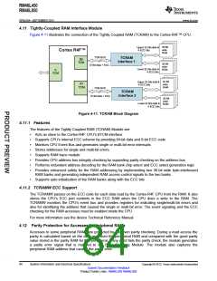
Figure 4-11 illustrates the connection of the Tightly Coupled RAM (TCRAM) to the Cortex-R4F™ CPU.
36 Bit
36 Bit
36 Bit
Upper 32 bits data &
4 ECC bits
wide
wide
wide
RAM
RAM
RAM
Cortex R4F™
TCM BUS
TCRAM
B0
TCM
36 Bit
36 Bit
36 Bit
Interface 1
wide
wide
wide
RAM
72 Bit data + ECC
RAM
RAM
Lower32 bits data &
4 ECC bits
A
TCM
36 Bit
36 Bit
36 Bwitide
wideRAM
RAM
RAM
Upper 32 bits data &
4 ECC bits
wide
B1
TCM
TCM BUS
TCRAM
Interface 2
36 Bit
36 Bit
72 Bit data + ECC
36 Bit
wide
wide
wide
RAM
RAM
RAM
Lower32 bits data &
4 ECC bits
Figure 4-11. TCRAM Block Diagram
4.11.1 Features
The features of the Tightly Coupled RAM (TCRAM) Module are:
•
•
•
•
•
•
•
•
Acts as slave to the Cortex-R4F CPU's BTCM interface
Supports CPU's internal ECC scheme by providing 64-bit data and 8-bit ECC code
Monitors CPU Event Bus and generates single or multi-bit error interrupts
Stores addresses for single and multi-bit errors
Supports RAM trace module
Provides CPU address bus integrity checking by supporting parity checking on the address bus
Performs redundant address decoding for the RAM bank chip select and ECC select generation logic
Provides enhanced safety for the RAM addressing by implementing two 36-bit wide byte-interleaved
RAM banks and generating independent RAM access control signals to the two banks
•
Supports auto-initialization of the RAM banks along with the ECC bits
4.11.2 TCRAMW ECC Support
The TCRAMW passes on the ECC code for each data read by the Cortex-R4F CPU from the RAM. It also
stores the CPU's ECC port contents in the ECC RAM when the CPU does a write to the RAM. The
TCRAMW monitors the CPU's event bus and provides registers for indicating single/multi-bit errors and
also for identifying the address that caused the single or multi-bit error. The event signaling and the ECC
checking for the RAM accesses must be enabled inside the CPU.
For more information see the device Technical Reference Manual.
4.12 Parity Protection for Accesses to peripheral RAMs
Accesses to some peripheral RAMs are protected by odd/even parity checking. During a read access the
parity is calculated based on the data read from the peripheral RAM and compared with the good parity
value stored in the parity RAM for that peripheral. If any word fails the parity check, the module generates
a parity error signal that is mapped to the Error Signaling Module. The module also captures the
peripheral RAM address that caused the parity error.
84
System Information and Electrical Specifications
Submit Documentation Feedback
Product Folder Links: RM46L450 RM46L850
Copyright © 2012, Texas Instruments Incorporated

 TI [ TEXAS INSTRUMENTS ]