RM46L450
RM46L850
www.ti.com
SPNS184 –SEPTEMBER 2012
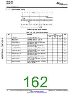
5.12.3 Management Data Input/Output (MDIO)
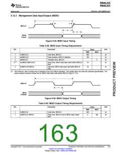
1
3
3
MDCLK
4
5
MDIO
(input)
Figure 5-25. MDIO Input Timing
Table 5-39. MDIO Input Timing Requirements
NO.
Parameter
Value
Unit
MIN
400
180
-
MAX
1
2
tc(MDCLK)
Cycle time, MDCLK
-
-
ns
ns
ns
ns
tw(MDCLK)
Pulse duration, MDCLK high/low
Transition time, MDCLK
3
4(1)
tt(MDCLK)
5
-
tsu(MDIO-MDCLKH)
Setup time, MDIO data input valid before MDCLK
High
10
5
th(MDCLKH-MDIO)
Hold time, MDIO data input valid after MDCLK
High
10
-
ns
(1) The minimum 10ns of setup time is dictated by the IEEE MDIO standard. This design does not meet this standard specification. The
actual required minimum setup time for MDIO data input valid before MDCLK high is 17 ns.
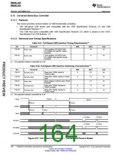
1
MDCLK
7
MDIO
(output)
Figure 5-26. MDIO Output Timing
Table 5-40. MDIO Output Timing Requirements
NO.
Parameter
Value
Unit
MIN
400
0
MAX
-
1
7
tc(MDCLK)
Cycle time, MDCLK
ns
ns
td(MDCLKL-MDIO)
Delay time, MDCLK low to MDIO data output
valid
100
Copyright © 2012, Texas Instruments Incorporated
Peripheral Information and Electrical Specifications
Submit Documentation Feedback
Product Folder Links: RM46L450 RM46L850
163

 TI [ TEXAS INSTRUMENTS ]