PGA400-Q1
SLDS186 –MARCH 2012
www.ti.com
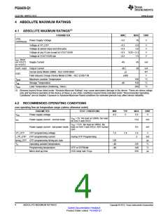
4 ABSOLUTE MAXIMUM RATINGS
4.1 ABSOLUTE MAXIMUM RATINGS(1)
PARAMETER
MIN
MAX
UNIT
VDD,
Power Supply Voltage
Continuous
–5.5
16
V
Voltage at VP_OTP
Voltage at sensor input and drive pins
Voltage at any IO pin except at VOUT1/OWI
Voltage at VOUT1/OWI pin
–0.3
–0.3
–0.3
–0.3
8.0
3.6
V
V
V
V
VDD + 0.3
7.5
IDD, Short
on VOUT1
or VOUT2
Supply Current
–45
–30
45
30
mA
Iout1, Iout2 Output Current
mA
KV
V
Human Body Model (HBM) - AEC-Q100-002D
±2
±500
ESD
Field Induced Charge Device Model (CDM) - AEC-Q100-11B
Maximum Junction Temperature
Tjmax
Tstg
150
150
260
°C
°C
°C
Storage Temperature
–40
Tlead
Lead Temperature (Soldering, 10sec)
(1) Stresses beyond those listed under “Absolute Maximum Ratings” may cause permanent damage to the device. These are stress ratings
only and functional operation of the device at these or any other conditions beyond those indicated under “Recommended Operating
Conditions” are not implied. Exposure to Absolute-Maximum-Rated conditions for extended periods may affect device reliability.
4.2 RECOMMENDED OPERATING CONDITIONS
over operating free-air temperature range (unless otherwise noted)
PARAMETER
TEST CONDITIONS
MIN
TYP
MAX
UNIT
VDD
IDD
Power supply voltage
4.5
5
5.5
V
VDD = 5V, No load on VBRG, No load
on DAC1 and DAC2
Power supply current - normal mode
13.6
mA
VDD = 5.5V, No load on VBRG, No
Power supply current - low power mode load on DAC1 and DAC2, AFE turned
OFF
9.5
mA
VP_OTP
OTP programming voltage
7.0
7.4
7.8
3
V
mA
µs
°C
°C
µs
I_VP_OTP
OTP programming current
During OTP Programming
tprog_OTP OTP programming timing per byte
120
–40
–40
TA
Operating ambient temperature
Programming temperature
Micro start-up time
125
140
250
OTP or EEPROM
VDD ramp rate 1V/µs
4
ABSOLUTE MAXIMUM RATINGS
Copyright © 2012, Texas Instruments Incorporated
Submit Documentation Feedback
Product Folder Link(s): PGA400-Q1

 TI [ TEXAS INSTRUMENTS ]