PGA400-Q1
www.ti.com
SLDS186 –MARCH 2012
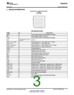
3 DEVICE INFORMATION
DIE-SIZE BALL GRID ARRAY (WCSP)
36 PINS
(TOP VIEW)
6
5
4
3
2
1
A
B
C
D
E
F
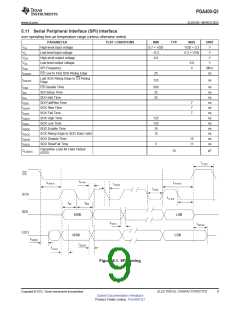
PIN DESCRIPTIONS
NAME
AVDD
CS
NO.
C6
F5
DESCRIPTION
Linear regulator output for internal analog circuit supply
Serial peripheral interface chip select
DVDD
F6
Linear regulator output for internal digital circuit supply
B2, B3, B5, B6, C3, C4, C5,
D5, E5, E6
GND
Ground
GPIO_1 / IC_1 / SDA
GPIO_2 / IC_2
GPIO_3 / OC_1/SCL
GPIO_4 / OC_2
GPIO_5
C2
D2
E3
D3
F1
A2
A5
F4
F3
D4
F2
E4
B1
D6
A3
A1
A6
A4
B4
D1
C1
E1
E2
General purpose IO 1 / input capture port 1 / I2C Data
General purpose IO 2 / input capture port 2
General purpose IO 3 / output compare port 1 / I2C Clock
General purpose IO 4 / output compare port 2
General purpose IO 5
ICAP1
Capactive sensor drive current 1
Capactive sensor drive current 2
Serial peripheral interface slave data out
Serial peripheral interface slave data in
8051 UART Rx (Port 3_0)
ICAP2
SDO
SDI
RXD
SCK
Serial Peripheral Interface clock
TXD
8051 UART Tx (Port 3_1)
VBRG
Resistive bridge supply voltage
VDD
Input power supply
VIN1N / CR1
VIN1P / CP1
VIN2N / CR2
VIN2P / CP2
VIN3
Resistive sensor 1 negative input / capacitive sensor 1 reference input
Resistive sensor 1 positive input / capacitive sensor 1 positive input
Resistive sensor 2 negative input / capacitive sensor 2 reference input
Resistive sensor 2 positive input / capacitive sensor 2 positive input
External temperature sensor input
VOUT1/OWI
VOUT2
DAC1 output / One-wire interface
DAC2 output
VP_OTP
XTAL
One-time programmable memory programming voltage
External crystal input
Copyright © 2012, Texas Instruments Incorporated
DEVICE INFORMATION
Submit Documentation Feedback
3
Product Folder Link(s): PGA400-Q1

 TI [ TEXAS INSTRUMENTS ]