PGA281
SBOS664A –MARCH 2013–REVISED JUNE 2013
www.ti.com
Electrical Overstress
Designers often ask questions about the capability of an amplifier to withstand electrical overstress. These
questions tend to focus on the device inputs, but may involve the supply voltage pins or even the output pin.
Each of these different pin functions have electrical stress limits determined by the voltage breakdown
characteristics of the particular semiconductor fabrication process and specific circuits connected to the pin.
Additionally, internal ESD protection is built into these circuits to protect them from accidental ESD events both
before and during product assembly.
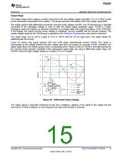
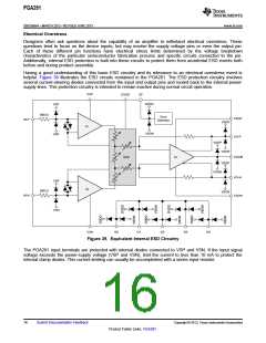
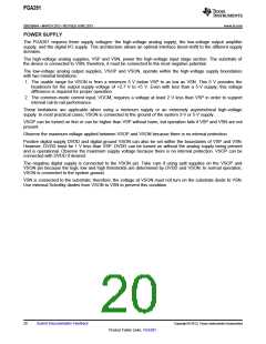
Having a good understanding of this basic ESD circuitry and its relevance to an electrical overstress event is
helpful. Figure 39 illustrates the ESD circuits contained in the PGA281. The ESD protection circuitry involves
several current-steering diodes connected from the input and output pins and routed back to the internal power-
supply lines. This protection circuitry is intended to remain inactive during normal circuit operation.
VSP
DVDD
EF
DVDD
VSP
600 W
Error
VSOP
VO-P
IN-P
Detection
VSOP
A1
VSON
VSN
VSOP
VSON
Gain
A3
VOCM
VSOP
VSON
VO-N
VSP
VSN
A2
600 W
VSON
IN-N
VSON
VSN
G0
G1
G2
G3
G4
Figure 39. Equivalent Internal ESD Circuitry
The PGA281 input terminals are protected with internal diodes connected to VSP and VSN. If the input signal
voltage exceeds the power-supply voltage (VSP and VSN), limit the current to less than 10 mA to protect the
internal clamp diodes. This current-limiting can usually be accomplished with a series input resistor.
16
Submit Documentation Feedback
Copyright © 2013, Texas Instruments Incorporated
Product Folder Links: PGA281

 TI [ TEXAS INSTRUMENTS ]