PGA281
SBOS664A –MARCH 2013–REVISED JUNE 2013
www.ti.com
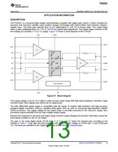
FUNCTIONAL BLOCKS
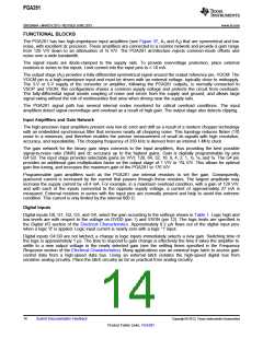
The PGA281 has two high-impedance input amplifiers (see Figure 37, A1 and A2) that are symmetrical and low
noise, with excellent dc precision. These amplifiers are connected to a resistor network and provide a gain range
from 128 V/V down to an attenuation of ⅛ V/V. The PGA281 architecture rejects common-mode offsets and
noise over a wide bandwidth.
The signal inputs are diode-clamped to the supply rails. To provide overvoltage protection, place external
resistors in series to the inputs. Limit current into the input pins to ≤ 10 mA.
The output stage (A3) provides a fully-differential symmetrical signal around the output reference pin, VOCM. The
VOCM pin is a high-impedance input and must be driven with an external voltage, typically close to midsupply.
The 3-V or 5-V supply of the converter or amplifier, following the PGA281 outputs, is normally connected to
VSOP and VSON; this configuration shares a common supply voltage and protects the circuit from overloads.
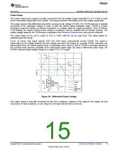
The fully-differential signal avoids coupling of noise and errors from the supply and ground, and allows large
signal swing without the risk of nonlinearities that arise when driving near the supply rails.
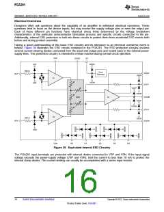
The PGA281 signal path has several internal nodes monitored for critical overload conditions. The input
amplifiers detect signal overvoltage and overload as a result of high gain. The output stage also detects clipping.
Input Amplifiers and Gain Network
The high-precision input amplifiers present very low dc error and drift as a result of a modern chopper technology
with an embedded synchronous filter that removes nearly all chopping noise. This topology reduces flicker (1/f)
noise to a minimum, and therefore enables the precise measurement of small dc-signals with high resolution,
accuracy, and repeatability. The chopping frequency of 250 kHz is derived from an internal 1-MHz clock.
The gain network for the binary gain steps connects to the input amplifiers, thus providing the best possible
signal-to-noise ratio (SNR) and dc accuracy up to the highest gains. Gain is digitally programmable by pins
G4:G0. The input stage provides selectable gains (in V/V): 128, 64, 32, 16, 8, 4, 2, 1, ½, ¼, and ⅛. The G4 pin
provides an additional gain multiplication factor on the output stage of 1 V/V or 1⅜ V/V. This allows for optimal
gain fine-tuning, and increases the maximum gain of the PGA281 to 176 V/V.
Programmable gain amplifiers such as the PGA281 use internal resistors to set the gain. Consequently,
quiescent current is increased by the current that passes through these resistors. The largest amplitude may
increase the supply current by ±0.4 mA. For example, in a maximum overload condition, with a gain of 128 V/V,
and with each of the inputs connected to the opposite supply voltage, a current of approximately 27 mA is
measured. External resistors in series with the input pins are normally present and help to avoid this extreme
condition. This current is only limited by the internal 600 Ω.
Digital Inputs
Digital inputs G0, G1, G2, G3, and G4, select the gain according to the settings shown in Table 1. Logic high and
low levels are with respect to the voltage on DVDD (pin 1) and VSON (pin 12). The logic limits are specified in
the Digital I/O section of the Electrical Characteristics. Approximately 0.2 µA flows out of the digital input pins
when a logic '0' is applied. Logic input current is nearly zero with a logic '1' input.
Digital inputs G4:G0 are not latched; a change in logic inputs immediately selects a new gain. Switching time of
the logic is approximately 1 µs. The time to respond to gain change is effectively the time it takes the amplifier to
settle to a new output voltage in the newly selected gain (see the settling times specified in the Frequency
Response section of the Electrical Characteristics). Many applications use an external logic latch to access gain
control data from a high-speed data bus. Using an external latch isolates the high-speed digital bus from
sensitive analog circuitry. Place the latch circuitry as far as practical from analog circuitry.
14
Submit Documentation Feedback
Copyright © 2013, Texas Instruments Incorporated
Product Folder Links: PGA281

 TI [ TEXAS INSTRUMENTS ]