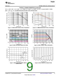
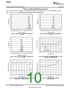
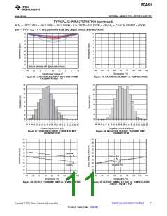
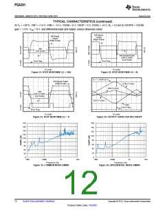
PGA281
www.ti.com
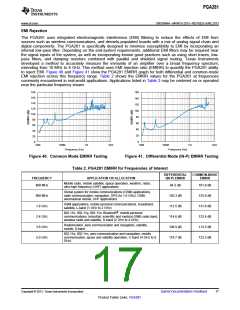
SBOS664A –MARCH 2013–REVISED JUNE 2013
APPLICATION INFORMATION
DESCRIPTION
The PGA281 is a universal high-voltage instrumentation amplifier with digital gain control. It offers excellent dc
precision and long-term stability using modern chopper technology with internal filters that minimize chopper-
related noise. The input gain extends from ⅛ V/V (attenuation) to 128 V/V in binary steps. The output stage
offers a gain multiplying factor of 1 V/V or 1⅜ V/V for optimal gain adjustment. The output stage connects to the
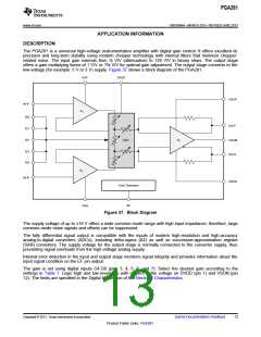
low-voltage (for example: 5 V or 3 V) supply. Figure 37 shows a block diagram of the PGA281.
VSP
DVDD
VSOP
IN-P
A1
G0
G1
G2
VO-P
Gain
A3
VOCM
VO-N
G3
G4
A2
IN-N
VSON
Error Detection
EF
VSN
Figure 37. Block Diagram
The supply voltage of up to ±18 V offers a wide common-mode range with high input impedance; therefore, large
common-mode noise signals and offsets can be suppressed.
The fully differential signal output is compatible with the inputs of modern high-resolution and high-accuracy
analog-to-digital converters (ADCs), including delta-sigma (ΔΣ) as well as successive-approximation register
(SAR) converters. The supply voltage for the output stage is normally connected to the converter supply, thus
preventing signal overloads from the high-voltage analog supply.
Internal error detection in the input and output stage monitors signal integrity and provides information about the
input signal condition on the EF pin output.
The gain is set using digital inputs G4:G0 (pins 3, 4, 5, 6, and 7). Select the desired gain according to the
settings in Table 1. Logic high and low levels are with respect to the voltage on DVDD (pin 1) and VSON (pin
12). The limits are specified in the Digital I/O section of the Electrical Characteristics.
Copyright © 2013, Texas Instruments Incorporated
Submit Documentation Feedback
13
Product Folder Links: PGA281

 TI [ TEXAS INSTRUMENTS ]