PGA281
www.ti.com
SBOS664A –MARCH 2013–REVISED JUNE 2013
Output Stage
The output stage power supply is usually connected to the low-voltage supply (normally 3 V or 5 V) that is used
by the subsequent signal path of the system. This design prevents overloading of the low-voltage signal path.
The output signal is fully differential around the common-mode voltage (VOCM). The VOCM input pin is typically
connected to the midsupply voltage in order to offer the widest signal amplitude range. VOCM is a high-
impedance input that requires an external connection to a voltage within the supply boundaries. If the VOCM pin
is left floating, the output common-mode voltage is undefined, and the amplifier will not operate properly. The
usable voltage range for the VOCM input is specified in the Electrical Characteristics and must be observed.
The output stage can be set to a gain of 1V/V or 1⅜V/V with the G4 pin logic level. This option allows for
additional gain fine tuning.
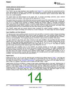
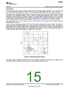
Figure 38 shows how signal outputs VOP and VON swing symmetrically around VOCM. The signal is
represented as the voltage between the two outputs and does not require an accurate VOCM. Therefore, the
signal output does not include ground noise or grounding errors. Noise or drift on VOCM is normally rejected by
the common-mode rejection capability of the subsequent signal stage. By using a differential output stage, the
PGA281 achieves large voltage swings on a single 3-V or 5-V supply.
5
4 VPP
4
3
2 VPP
2
1
15 V
5 V
0
-1
-2
VOP
VOCM
VOP
VOCM
PGA281
G = 1/4
8 VPP
VON
+2.5 V
VON
Differential
VOUT
-15 V
C037
Figure 38. Differential Output Voltage
The output signal is internally monitored for two error conditions: clipping of the signal to the supply rail and
overcurrent. In fault conditions, an error flag bit is set high until the fault is removed.
Copyright © 2013, Texas Instruments Incorporated
Submit Documentation Feedback
15
Product Folder Links: PGA281

 TI [ TEXAS INSTRUMENTS ]