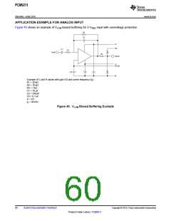
PCM9211
SBAS495 –JUNE 2010
www.ti.com
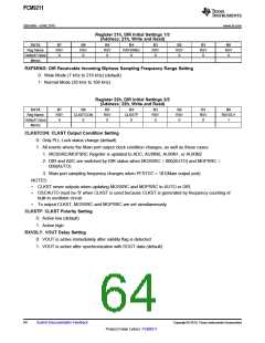
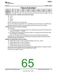
Register 21h, DIR Initial Settings 1/3
(Address: 21h, Write and Read)
DATA
Reg Name
Default Value
Memo
B7
RSV
0
B6
RSV
0
B5
RSV
0
B4
RXFSRNG
0
B3
RSV
0
B2
RSV
0
B1
RSV
0
B0
RSV
0
RXFSRNG: DIR Receivable Incoming Biphase Sampling Frequency Range Setting
0: Wide Mode (7 kHz to 216 kHz) (default)
1: Normal Mode (28 kHz to 108 kHz)
spacer
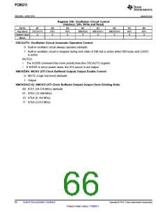
Register 22h, DIR Initial Settings 2/3
(Address: 22h, Write and Read)
DATA
Reg Name
Default Value
Memo
B7
RSV
0
B6
CLKSTCON
0
B5
RSV
0
B4
CLKSTP
0
B3
RSV
0
B2
RSV
0
B1
RSV
0
B0
RXVDLY
1
CLKSTCON: CLKST Output Condition Setting
0: Only PLL Lock status change (default)
1: All events where the Main port output clock condition changes, as well as these cases:
1. MOSSRC/MOPSRC Register is updated to ADC, AUXIN0, AUXIN1, or AUXIN2
2. DIR and ADC are switched by DIR status when MOSSRC = 000(AUTO) and MOPSRC =
000(AUTO)
3. Main port sampling frequency changes when PFSTGT = 101(Main output port)
NOTES:
•
•
CLKST never outputs when updating MOSSRC and MOPSRC to AUTO or DIR.
OSCAUTO must be '0' when CLKST is used because CLKST is generated by frequency counting of
built-in oscillator circuit.
•
To output CLKST, MOSSRC and MOPSRC are set simultaneously.
CLKSTP: CLKST Polarity Setting
0: Active low (default)
1: Active high
RXVDLY: VOUT Delay Setting
0: VOUT is active immediately after validity flag is detected
1: VOUT is active after synchronization with DOUT data (default)
64
Submit Documentation Feedback
Copyright © 2010, Texas Instruments Incorporated
Product Folder Link(s): PCM9211

 TI [ TEXAS INSTRUMENTS ]