PCM9211
www.ti.com
SBAS495 –JUNE 2010
Register Write Operation
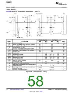
Figure 37 shows the functional timing diagram for a single write operation on the serial control port. MS is held at
'1' until a register must be written. To start the register write cycle, MS should be set to '0'. 16 clocks are then
provided on MC, corresponding to the 16 bits of the control data word on MDI. After the 16th clock cycle has
been completed, MS is set to '1' to latch the data into the indexed mode control register.
MS
MC
DC
“ 0” ADR 6 ADR 5 ADR 4 ADR 3 ADR
2
ADR 1 ADR 0 D7
D6
D5
D4
D3
D2
D1
D0
DC
DC R /W ADR 6
MDI
Figure 37. Register Write Operation
Channel status data are available from the Channel Status registers. To read the first 48 bits of the Channel
Status registers accurately, the read should be started 48fS after the start of the block. However, once MS is
pulled to '0', there are no time requirements in which to read the data because the registers are locked.
Both INT0 and INT1 can also be masked to highlight when the Channel Status has been updated. In many
cases, Channel Status does not change during playback (of a movie or music). Once the source changes,
though, the Channel Status changes. This change causes an interrupt, which can then be used to trigger the
DSP to read the Channel Status registers. The interrupt source is called OCSRNWx (Output Channel Status
Renewal).
The OCSRNWx flag can be held in the INTx register, or masked and brought out to the ERR/INT0 or
NPCM/INT1 pin.
Register Read Operation
Figure 38 shows the functional timing diagram for single read operations on the SPI serial control port. MS is
held high until a register is to be read. To start the register read cycle, MS is set to a low state. 16 clocks are
then provided on MC, corresponding to the first eight bits of the control data word on MDI, and second eight bits
of the read-back data word from MDO. After the 16th clock cycle has been completed, MS is set to high for next
write or read operation. MDO remains in a Hi-Z (or high impedance) state except for a period of eight MC clocks
for actual data transfer.
MS
MC
DC
“1 ”
R /W
ADR 6
MDI
ADR 6 ADR 5 ADR 4 ADR 3 ADR 2 ADR 1 ADR 0
DON ’T CARE (DC)
“HI - Z”
D7
D6
D5
D4
D3
D2
D1
D0
“HI -Z”
MDO
Figure 38. Register Read Operation
Copyright © 2010, Texas Instruments Incorporated
Submit Documentation Feedback
55
Product Folder Link(s): PCM9211

 TI [ TEXAS INSTRUMENTS ]