PCM9211
www.ti.com
SBAS495 –JUNE 2010
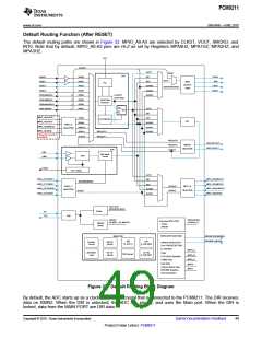
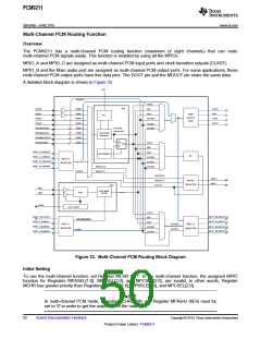
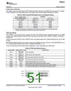
Output Source Selection
The output source for Multi-Channel PCM Output (the Main output port and MPIO_B) is selected by a register.
Table 29 describes the relationship between the output source and the register (MCHRSRC) setting.
Table 29. Multi-Channel PCM Output Source and Register Setting
MCHRSRC
MULTI-CHANNEL MODE
OUTPUT SOURCE SELECT
CLOCK SOURCE
DOUT
'00' or '10'
'01' or '11'
MULTI-CH INPUT
MDIN0
(1)
MAIN OUT
MAIN OUT
MAIN OUT
Logic low
Logic low
Logic low
(1)
(1)
MDOUT0
MDIN0
MDOUT1
MDIN1
MDOUT2
MDIN2
MDOUT3
MDIN3
(1) The Main OUT data source is discussed in the DIR section of this data sheet. It can either be the DIR
recovered clock and data, or the ADC DATA and the ADC clock source.
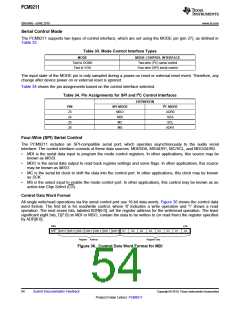
DSD Input Mode
The PCM9211 can also be used to suppress the jitter of the DSCKI signals, typically generated by an HDMI
receiver. DSD signals (DBCKI, DSDRI, DSDLI) are routed to the Main Port as DBCKO, DSDRO, and DSDLO,
respectively.
The DIT works with DSCKI for SCK, DBCKI for BCK, internally-created LRCK, DBCKI divided by 64, and '0' data
for DIN.
MOLRMTEN (Register 6Ah) can be used to mute/unmute DSDRO from the LRCK port. When MOLRMTEN is set
to '1', mute/unmute of DSDRO from LRCK is available by MODMUT = 1/0.
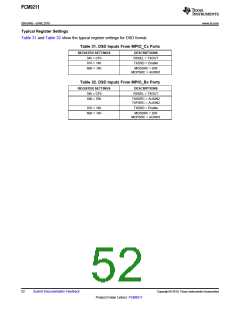
Table 30 summarizes the DSD input mode configuration. Figure 34 illustrates the DSD format.
Table 30. DSD Input Mode Summary
SIGNAL NAME
MPIO GROUP / PIN
DESCRIPTION
MPIO_C0 or
MPIO_B0
DSCKI
SCK input (256fS)
MPIO_C1 or
MPIO_B1
DBCKI
DSDRI
DSDLI
DBCK input for DSD format (64fS)
MPIO_C2 or
MPIO_B2
R-channel DSD data input for DSD format
L-channel DSD data input for DSD format
MPIO_C3 or
MPIO_B3
DSCKO
DBCKO
DSDRO
DSDLO
SCKO
BCK
SCK output generated by DIR from DIT output
DBCK output for DSD format (the same signal as DBCKI)
R-channel DSD data output for DSD format (the same signal as DSDRI)
L-channel DSD data output for DSD format(the same signal as DSDLI)
LRCK
DOUT
DBCK
DSDRI
DSDLI
1
1
2
2
3
3
62 63 64
62 63 64
1
1
2
2
3
3
Figure 34. DSD Format
Copyright © 2010, Texas Instruments Incorporated
Submit Documentation Feedback
51
Product Folder Link(s): PCM9211

 TI [ TEXAS INSTRUMENTS ]