PCM9211
SBAS495 –JUNE 2010
www.ti.com
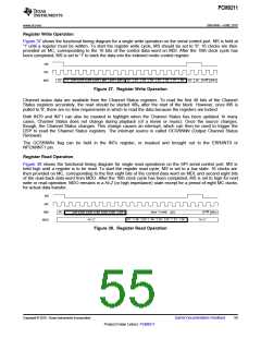
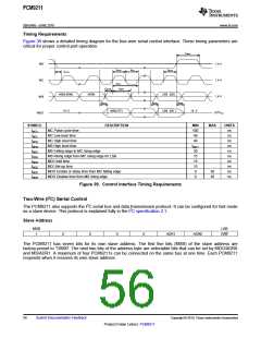
Timing Requirements
Figure 39 shows a detailed timing diagram for the four-wire serial control interface. These timing parameters are
critical for proper control port operation.
t MHH
MS
MC
1.4 V
1.4 V
tMCH
tMCL
t MS H
tM S S
tMCY
tMDH
tMDS
MSB (R/W)
ADR0
LSB (D0)
1.4 V
MDI
MDO
tMD D
tM DD
t MDR
Hi -Z
MSB (D7)
LSB (D0 )
Hi -Z
0.5*VDD
SYMBOL
tMCY
DESCRIPTION
MIN
100
40
40
tMCY
30
15
15
15
0
MAX
UNITS
ns
MC Pulse cycle time
MC Low level time
MC High level time
MS High level time
tMCL
ns
tMCH
tMHH
tMSS
ns
ns
MS Falling edge to MC rising edge
ns
tMSH
MS Rising edge from MC rising edge for LSB
MDI Hold time
ns
tMDH
tMDS
tMDD
tMDR
ns
MDI Set-up time
ns
MDO Enable or delay time from MC falling edge
MDO Disable time from MS rising edge
30
30
ns
0
ns
Figure 39. Control Interface Timing Requirements
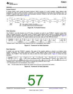
Two-Wire (I2C) Serial Control
The PCM9211 also supports the I2C serial bus and data transmission protocol. It can be configured for fast mode
as a slave device. This protocol is explained fully in the I2C specification 2.1.
Slave Address
MSB
1
LSB
R/W
0
0
0
0
ADR1
ADR0
The PCM9211 has seven bits for its own slave address. The first five bits (MSB) of the slave address are
factory-preset to '10000'. The next two bits of the address byte are selectable bits that can be set by MDO/ADR0
and MS/ADR1. A maximum of four PCM9211s can be connected on the same bus at one time. Each PCM9211
responds when it receives its own slave address.
56
Submit Documentation Feedback
Copyright © 2010, Texas Instruments Incorporated
Product Folder Link(s): PCM9211

 TI [ TEXAS INSTRUMENTS ]