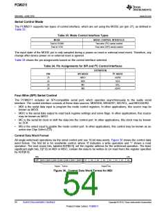
PCM9211
SBAS495 –JUNE 2010
www.ti.com
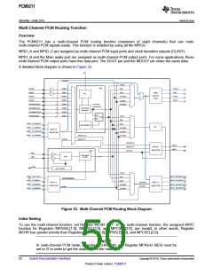
Multi-Channel PCM Routing Function
Overview
The PCM9211 has a multi-channel PCM routing function (maximum of eight channels) that can route
multi-channel PCM signals easily. This function is enabled by using all the MPIOs.
MPIO_A and MPIO_C are assigned as multi-channel PCM input ports and clock transition outputs (CLKST).
MPIO_B and the Main audio port are assigned as multi-channel PCM output ports. For some applications, these
multi-channel PCM output ports have five data pins. The DOUT pin and the MDOUT pin share the same data.
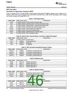
A detailed block diagram is shown in Figure 33.
FILT
AUXIN 0
AUTO
DIR
RXIN0
RXIN0
RXIN1
RXIN2
RXIN3
RXIN4
DIR
SCKO
BCK
RXIN1
ADC
MAIN
PLL
OUTPUT
PORT
RXIN2
AUXIN0
LRCK
DOUT
RXIN3
AUXIN1
AUXIN2
RXIN4/ASCKI0
Lock:DIR
Unlock:ADC
RXIN5/ABCKI0
RXIN6/ALRCKI 0
RXIN7/ADIN0
RXIN5
RXIN6
RXIN7
Clock/ Data
Recovery
AUTO
DIR
MPIO _A0 (MSCKI)
MPIO _A1 (MBCKI)
MPIO _A2 (MLRCKI)
MPIO _A3 (MDIN0)
ADC
Lock Detection
DIT
AUXIN0
AUXIN1
AUXIN2
MPIO_A
SELECTOR
RECOUT0
RECOUT1
DITOUT
RECOUT0
RECOUT1
DITOUT
MPO 0
MPO 1
MPO0/1
SELECTOR
ADC
VINL
VINR
ADC Mode
Control
ADC
VCOM
Com. Supply
AUTO
DIR
MPIO _C0(CLKST)
MPIO _C1(MDIN1)
MPIO _C2(MDIN2)
MPIO _C3(MDIN3)
MPIO_B0 (MDOUT 0)
MPIO_B1 (MDOUT 1)
ADC Standalone
ADC
MPIO_C
AUXOUT
AUXIN 2
MPIO _B
MPIO_B2 (MDOUT 2)
MPIO_B3 (MDOUT 3)
AUXIN0
AUXIN1
SELECTOR
SELECTOR
AUXIN1
Figure 33. Multi-Channel PCM Routing Block Diagram
Initial Setting
To use the multi-channel function, set Register MCHR to '1'. In the multi-channel function, the assigned MPIO
function for Registers MPASEL[1:0], MPBSEL[2:0], and MPCSEL[2:0], are invalid; in other words, Register
MCHR has greater priority than Registers MPASEL[1:0], MPBSLE[2:0], and MPCSEL[2:0].
NOTE
In multi-channel PCM mode, Register MCHR (20h) and Register MPAxHz (6Eh) must be
set to '0' in order to get the outputs from the main port.
50
Submit Documentation Feedback
Copyright © 2010, Texas Instruments Incorporated
Product Folder Link(s): PCM9211

 TI [ TEXAS INSTRUMENTS ]