PCM9211
SBAS495 –JUNE 2010
www.ti.com
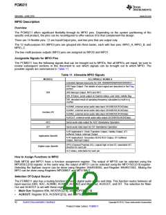
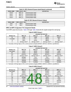
MPIO Description
Description for Signal Name Assigned to MPIO
Table 17 through Table 25 list the details of where each of the internal PCM9211 signals can be routed to. For
instance, DIR LOCK can be output to any of the MPIO and MPO pins, while SBCK (Secondary Clock Output)
can only be brought out through MPIO_A0.
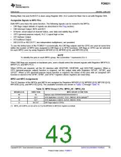
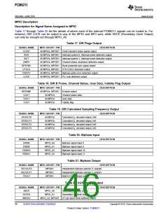
Table 17. DIR Flags Output
SIGNAL NAME
CLKST
INT0
MPIO GROUP / PIN
DESCRIPTION
All MPIOs, MPO0/1 Clock transient status signal output
All MPIOs, MPO0/1 Interrupt system 0, Interrupt event detection output
All MPIOs, MPO0/1 Interrupt system 1, Interrupt event detection output
All MPIOs, MPO0/1 Channel status, emphasis detection output
All MPIOs, MPO0/1 Burst preamble sync signal output
All MPIOs, MPO0/1 DTS-CD/LD detection output
INT1
EMPH
BPSYNC
DTSCD
PARITY
LOCK
All MPIOs, MPO0/1 Biphase parity error detection output
All MPIOs, MPO0/1 PLL lock detection output
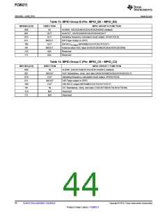
Table 18. DIR B Frame, Channel Status, User Data, Validity Flag Output
SIGNAL NAME
BFRAME
COUT
MPIO GROUP / PIN
DESCRIPTION
All MPIOs, MPO0/1 B frame output
All MPIOs
All MPIOs
All MPIOs
Channel status data
UOUT
User data
VOUT
Validity flag
Table 19. DIR Calculated Sampling Frequency Output
SIGNAL NAME
SFSOUT0
MPIO GROUP / PIN
DESCRIPTION
All MPIOs
All MPIOs
All MPIOs
All MPIOs
Calculated fS, decoded output, bit0
Calculated fS, decoded output, bit1
Calculated fS, decoded output, bit2
Calculated fS, decoded output, bit3
SFSOUT1
SFSOUT2
SFSOUT3
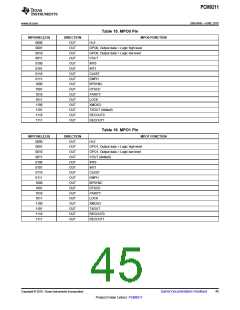
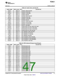
Table 20. Biphase Input
SIGNAL NAME
RXIN8
MPIO GROUP / PIN
MPIO_A0
DESCRIPTION
Biphase signal input 8
Biphase signal input 9
Biphase signal input 10
Biphase signal input 11
RXIN9
MPIO_A1
RXIN10
MPIO_A2
RXIN11
MPIO_A3
Table 21. Biphase Output
SIGNAL NAME
RECOUT0
RECOUT1
TXOUT
MPIO GROUP / PIN
MPO0/1
DESCRIPTION
Independent biphase selector 0, output0
Independent biphase selector 1, output1
Built-in DIT, biphase output
MPO0/1
MPO0/1
Table 22. AUX Clocks Output
SIGNAL NAME
SBCK
MPIO GROUP / PIN
MPIO_A0
DESCRIPTION
Secondary bit clock output
Secondary LR clock output
SLRCK
MPIO_A1
XMCKO
MPIO_A2, MPO0/1 XTI pin input clock buffered output
46
Submit Documentation Feedback
Copyright © 2010, Texas Instruments Incorporated
Product Folder Link(s): PCM9211

 TI [ TEXAS INSTRUMENTS ]