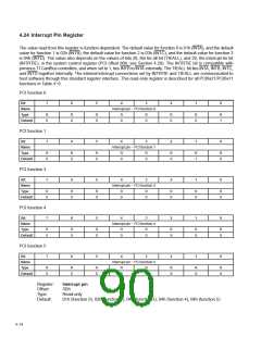
4.24 Interrupt Pin Register
The value read from this register is function dependent. The default value for function 0 is 01h (INTA), and the default
value for function 1 is 02h (INTB), the default value for function 2 is 03h (INTC), and the default value for function 3
is 04h (INTD). The value also depends on the values of bits 28, the tie-all bit (TIEALL), and 29, the interrupt tie bit
(INTRTIE), in the system control register (PCI offset 80h, see Section 4.29). The INTRTIE bit is compatible with
previous TI CardBus controllers, and when set to 1, ties INTB to INTA internally. The TIEALL bit ties INTA, INTB, INTC,
and INTD together internally. The internal interrupt connections set by INTRTIE and TIEALL are communicated to
host software through this standard register interface. This read-only register is described for all PCI6x21/PCI6x11
functions in Table 4−6.
PCI function 0
Bit
7
6
5
4
3
2
1
0
Name
Type
Default
Interrupt pin − PCI function 0
R
0
R
0
R
0
R
0
R
0
R
0
R
0
R
1
PCI function 1
Bit
7
6
5
4
3
2
1
0
Name
Interrupt pin − PCI function 1
Type
R
0
R
0
R
0
R
0
R
0
R
0
R
1
R
0
Default
PCI function 3
Bit
7
6
5
4
3
2
1
0
Name
Interrupt pin − PCI function 3
Type
R
0
R
0
R
0
R
0
R
0
R
X
R
X
R
X
Default
PCI function 4
Bit
7
6
5
4
3
2
1
0
Name
Interrupt pin − PCI function 4
Type
R
0
R
0
R
0
R
0
R
0
R
X
R
X
R
X
Default
PCI function 5
Bit
7
6
5
4
3
2
1
0
Name
Interrupt pin − PCI function 5
Type
R
0
R
0
R
0
R
0
R
0
R
X
R
X
R
X
Default
Register:
Offset:
Type:
Interrupt pin
3Dh
Read-only
Default:
01h (function 0), 02h (function 1), 04h (function 3), 04h (function 4), 04h (function 5)
4−14

 TI [ TEXAS INSTRUMENTS ]