Table 4−3. Command Register Description (continued)
BIT
SIGNAL
TYPE
FUNCTION
Memory space enable. This bit controls whether or not the PCI6x21/PCI6x11 controller can claim cycles
in PCI memory space.
1
MEM_EN
RW
RW
0 = Disables the PCI6x21/PCI6x11 response to memory space accesses (default)
1 = Enables the PCI6x21/PCI6x11 response to memory space accesses
I/O space control. This bit controls whether or not the PCI6x21/PCI6x11 controller can claim cycles in PCI
I/O space.
0
IO_EN
0 = Disables the PCI6x21/PCI6x11 controller from responding to I/O space accesses (default)
1 = Enables the PCI6x21/PCI6x11 controller to respond to I/O space accesses
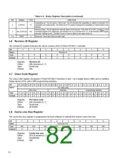
4.5 Status Register
The status register provides device information to the host system. Bits in this register can be read normally. A bit
in the status register is reset when a 1 is written to that bit location; a 0 written to a bit location has no effect. All bit
functions adhere to the definitions in the PCI Bus Specification, as seen in the bit descriptions. PCI bus status is shown
through each function. See Table 4−4 for a complete description of the register contents.
Bit
15
14
13
12
11
10
9
8
7
6
5
4
3
2
1
0
Name
Type
Default
Status
RW
0
RW
0
RW
0
RW
0
RW
0
R
0
R
1
RW
0
R
0
R
0
R
0
R
1
RU
0
R
0
R
0
R
0
Register:
Offset:
Type:
Status
06h (Functions 0, 1)
Read-only, Read/Write
0210h
Default:
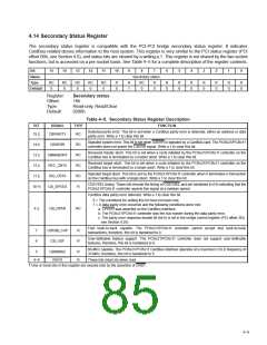
Table 4−4. Status Register Description
BIT
SIGNAL
TYPE
FUNCTION
Detected parity error. This bit is set when a parity error is detected, either an address or data parity error.
Write a 1 to clear this bit.
15 ‡
PAR_ERR
RW
Signaled system error. This bit is set when SERR is enabled and the PCI6x21/PCI6x11 controller signaled
a system error to the host. Write a 1 to clear this bit.
14 ‡
13 ‡
12 ‡
11 ‡
10−9
SYS_ERR
MABORT
RW
RW
RW
RW
R
Received master abort. This bit is set when a cycle initiated by the PCI6x21/PCI6x11 controller on the PCI
bus has been terminated by a master abort. Write a 1 to clear this bit.
Received target abort. This bit is set when a cycle initiated by the PCI6x21/PCI6x11 controller on the PCI
bus was terminated by a target abort. Write a 1 to clear this bit.
TABT_REC
TABT_SIG
PCI_SPEED
Signaled target abort. This bit is set by the PCI6x21/PCI6x11 controller when it terminates a transaction on
the PCI bus with a target abort. Write a 1 to clear this bit.
DEVSEL timing. These bits encode the timing of DEVSEL and are hardwired to 01b indicating that the
PCI6x21/PCI6x11 controller asserts this signal at a medium speed on nonconfiguration cycle accesses.
Data parity error detected. Write a 1 to clear this bit.
0 = The conditions for setting this bit have not been met.
1 = A data parity error occurred and the following conditions were met:
a. PERR was asserted by any PCI device including the PCI6x21/PCI6x11 controller.
b. The PCI6x21/PCI6x11 controller was the bus master during the data parity error.
c. The parity error response bit is set in the command register.
8 ‡
DATAPAR
RW
Fast back-to-back capable. The PCI6x21/PCI6x11 controller cannot accept fast back-to-back transactions;
thus, this bit is hardwired to 0.
7
6
5
FBB_CAP
UDF
R
R
R
UDF supported. The PCI6x21/PCI6x11 controller does not support user-definable features; therefore, this
bit is hardwired to 0.
66-MHz capable. The PCI6x21/PCI6x11 controller operates at a maximum PCLK frequency of 33 MHz;
therefore, this bit is hardwired to 0.
66MHZ
‡
One or more bits in this register are cleared only by the assertion of GRST.
4−5

 TI [ TEXAS INSTRUMENTS ]